Erik Bakkers and the three nanowire revolutions
His laboratory may well realize the world’s first Majorana qubits, the essential ingredient for a superior quantum computer, within a decade or so. But Erik Bakkers’ nanowire research is set to revolutionize the semiconductor world much earlier, via a different path. He is doing what was thought to be impossible: adapting the basic semiconductor feedstock– silicon – such that it can emit light. This can become the much sought key to integrating photonics and its many advantages into microelectronics. And by the way: Bakkers (1972) also has a nanowire revolution up his sleeves for solar cells.
Navigate to the three research fields of Erik Bakkers via the buttons below, or scroll down to read the whole article.
The story of Erik Bakkers and his nanowires starts at the Natlab research facility of the electronics multinational Philips. This illustrious research center, established in 1914 and breeding ground of many new technologies, hired Bakkers right after he gained his PhD. The electronics company more or less gave him carte blanche. Bakkers got the assignment to identify new and promising research fields and to pick the most promising one. His study led him to ‘nanowires’. It was a field that was still in its infancy, only ten years old.
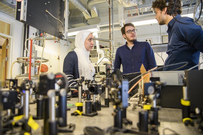
That turned out to be the right choice. Nanowire research has exploded, and within this area Bakkers has grown to be one of world’s finest experts on growing nanowires. He now heads a research group at Eindhoven University of Technology. His specialty is ‘materials’: he can meticulously control the growth of the nanowire crystal structure, which is the key to much wanted new materials and characteristics. It is a specialty, says Bakkers, that requires a lot of top notch science and engineering, but “also intuition is very important”.
MAJORANA
Majorana-research is one of the key topics of Bakkers’ group at Eindhoven University of Technology. Majorana fermions are quasi-particles whose existence was predicted in the 1930’s by Italian physicist Ettore Majorana, but so far nobody found them. For decades, there was no progress, but in 2012 there was a breakthrough. Bakkers and fellow professor Leo Kouwenhoven from Delft University of Technology got worldwide attention with their Science publication about the first signs of Majorana’s, detected in nanowires that were created in Bakkers’ lab.
It looked like just a matter of time before the first Majorana’s would be exposed, but material problems stood in the way. “It took us five years before we could do the next series of measurements”, Bakkers tells. “Our set-up is to create Majorana’s in a semiconductor nanowire with a superconductor on top of it. The quality of the interface between the two materials has turned out to be crucial. This should be extremely clean without any disorder. It took some time, but we solved that issue, here in Eindhoven.”
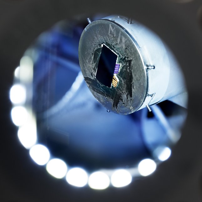
In 2017, the research consortium published a paper in Nature, based on a newly developed device: a double nanowire cross, also dubbed the ‘nano-hashtag’. This structure could one day become the first Majorana qubit, the building block of a quantum computer. But it was still not the definitive proof.
For Bakkers the slow progress was a sign that maybe they were not working with the right materials. So far, the experiments were based on a semiconductor nanowire made out indium-antimonide, topped with aluminum superconductor. “We have tried it with these materials for six years, but our progress is too slow”, says Bakkers. “It is not clear if the current materials are good enough for hosting Majorana’s and Majorana braiding, which is the ultimate proof. We are therefore going to explore new, more extreme materials. We are going to use lead telluride as semiconductor, and lead as superconductor – which is a stronger superconductor than aluminum. With this combination we can increase the energy scales of the system and with that the stability.” This idea gained him a 2.5 million euros Advanced Grant from the European Research Council, early 2019.
Ultimate proof
Bakker’s nanowires have become more and more pivotal in Majorana research. At first he and his team ‘only’ did the nanowires. The superconductor and the contacts were added in Santa Barbara and Delft respectively, and the actual experiments were done in Delft. But for quite some years now Bakkers’ lab has also been adding the superconductor, which saves the device a transoceanic trip and all due risks.
Since recently the contacts are also added in Eindhoven, which means Bakkers team now has the unique capacity to produce the entire device that is required to do Majorana research. And Bakkers, as before, is supplying his products to several scientists worldwide, for example in China and the US, and in Delft. Which leads to the question: why doesn’t he do the Majorana experiments himself, in Eindhoven? “That is exactly what we have set out to do”, says Bakkers with a smile. “These experiments are difficult and require large cryostats that can cool down a sample to just 10 millikelvin above absolute zero. With my new ERC-grant, I am going to build just such a set-up.”
So the world’s first Majorana’s fermions may be detected in Eindhoven? It is a question that the professor does not want to speculate on. “By supplying other scientists with our nano-hashtags, we are hedging our bets. So when the existence of Majorana fermions is proven, it may very well be on one of my devices”, Bakkers explains his strategy. “But it is not going to happen tomorrow. I think it will take some ten years before science can definitively demonstrate the ultimate proof of Majorana fermions: Majorana braiding. And realizing the first fully functional Majorana quantum computer will take at least ten years more.” Which, by the way, is not his primary goal. “For me, the quest for Majorana’s is mainly a way to do exciting, ground-breaking science”, Bakkers says with a grin.
LIGHT FROM SILICON
Majorana’s are hot news, they are elusive, they are exciting particle physics and they are the basis for a superior quantum computer. Still, Bakkers has another research line that gets him even more excited than his work on Majorana’s. The Eindhoven researcher and his team are on their way to create a silicon-germanium microlaser. “That will truly be a major breakthrough. It will be a game-changer, an invention that could transform the microelectronics industry”, Bakkers explains.
This industry, which has a multi-hundred billion euro market size, is largely based on silicon. It is the main semiconductor material that computer chips are made of. One of the keywords in the progress of microelectronics is integration, which is why chips are officially called ‘integrated circuits’, or ICs. Chips integrate an ever increasing amount of functions and with that more and more components. Nowadays ICs consist of up to billions of components, of ever smaller sizes. The data processing and storage capacities of microchips have continuously grown at high pace over the last decades.
But there is one thing in which electronics hasn’t excelled equally: data transfer. That is why data communication is gradually shifting from electronics to photonics; the use of light. This requires nanolasers to generate light signals, and preferably such that they can be integrated in the microelectronics architecture. And this is where the problem arises: it is impossible to let silicon emit light. Therefore photonic chips are currently made with other semiconductor materials, materials that do have the capacity to emit light. Unfortunately these materials, like indiumphosphide, are incompatible with silicon. So it was thought to be impossible to integrate lasers in microelectronics.
Hexagonal silicon
But with the work done in Erik Bakkers’ lab, it may soon become possible. He is getting light out of a silicon alloy, silicon germanium, and he is progressing fast. How he did it? By creating a new type of silicon. Silicon atoms by nature line up in a cubic crystal pattern. However, theoretical calculations predicted that silicon crystal in which atoms are arranged hexagonally, can emit light. The crux is in the gap between two top electron bands of silicon atoms, the so-called band gap. If an electron ‘drops’ from the conductance band to the valence band, it emits a photon: light. Unless the conductance band and the valence band are too close, which is the case in silicon, so it has no band gap, and therefore no photons are emitted. But hexagonal silicon does have a band gap.
So Bakkers and his team first set out to create hexagonal silicon – by using nanowires. In 2015, they succeeded. They created very pure hexagonal silicon by first growing nanowires of another material, with a hexagonal crystal structure. Then they grew a silicon shell on those nanowires. They were able to do this such that the silicon atoms built on, and continued the hexagonal structure.
That was a feat in itself, but the next step was more thrilling. Does the new material also emit light? It turned out: it does. Bakkers: “We are seeing light emissions at exactly the energy levels as predicted. It shifts frequency if we add germanium, which gives us a tunable direct bandgap from 2 to 3.5 micrometer. This is important, because you need multiple light frequencies to allow for simultaneous transmission of several signals via one and the same optical fiber.”
Creating a laser now is a matter of time, Bakker thinks. “By now we have realized optical properties which are almost comparable to indium phosphide and gallium arsenide, and the materials quality is steeply improving. If things run smooth, we can create a silicon laser in 2020.” In the meantime his team is also investigating how to integrate the hexagonal silicon in cubic silicon microelectronics, which would be the final piece of this work.
“If this works out, we have successfully added photonic capabilities to electronics. That will revolutionize the microelectronics industry, by adding intra-chip and chip-to-chip optical communication, which requires much less energy and generates much less heat. This is important because this will help put a brake on the soaring energy consumption of microelectronics.” Intra-chip optical communication will also result in faster chips; the current speed of chips is limited by the resistance of the copper lines connecting the many transistors on a chip. By using light, which has no resistance, the clock frequency can be enormously increased.
SOLAR CELLS
Bakkers’ nanowires may not only revolutionize computing, but also become a key element in sustainable energy supply. Bakkers thinks that within a few years he can break the Shockley-Queisser limit. This is the theoretical maximum efficiency of solar cells which was first calculated in 1961, and it still holds. It states that due to physical laws, solar panels can only convert about one third of the sun light they absorb into electricity. But Bakkers is convinced that his nanowire solar cells can go beyond this limit.
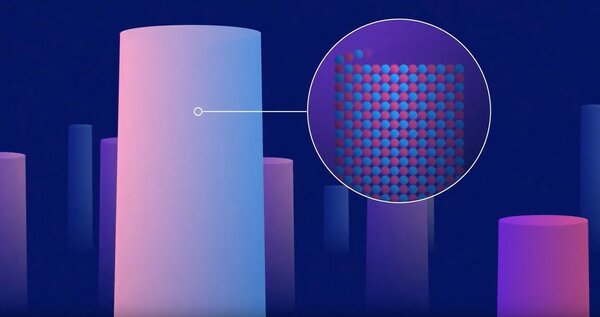
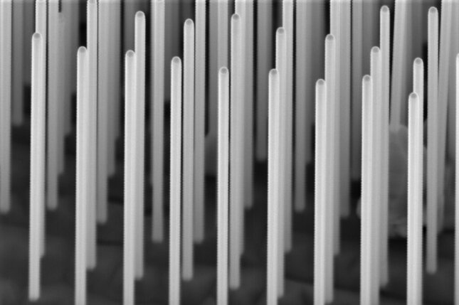
Worldwide, there is a massive amount of research on solar cells, of different technologies. Nanowire solar cells are a relatively new technology, it emerged about fifteen years ago. The nanowire cells are not composed of solid, flat layers, as is the case in most other technologies. They comprise a ‘lawn’ of vertical wires of each around two hundred nanometers thick, which is 300 times thinner than a human hair.
The record efficiencies achieved with nanowires are progressing at a much higher speed than the efficiencies of other solar cell technologies, so it is a very promising path. In 2016, Bakkers’ group set the world record efficiency for nanowire solar cells at 17.8 percent. How come that nanowire solar cells perform so well? The answer mainly lies in the dimensions of the nanowires. Because of their size, nanowires act as a kind of antenna that capture the light. Another factor that contributes to the performance of the nanowire cell is that they concentrate the light. The diameter of the nanowires determines how well the light is concentrated.
Reaching above the Shockley-Queisser limit, which is about 33 percent “would be spectacular by itself”, Bakkers says. “I think many research groups will jump on this, and this surge of new research will lead to an important increase of solar cell efficiency.”
“We want to reach this by reducing entropy losses. These have been included in the Shockley-Queisser theory of 1961, but have been forgotten by most people. By using the nanowire geometry, we think we can reduce these losses, due to the fact that this geometry can guide the lightwaves. It will not be straightforward to demonstrate this. The key element is the quality and hence the internal efficiency of the material, that should be excellent. That is exactly what we are good at.”
Are you looking for more information?
THE QUANTUM REVOLUTION
Are you interested in the research on new quantum technologies? Would you like to work - together with our scientists - on the 'quantum revolution'? Explore what Eindhoven University of Technology has to offer you.