Netherlands tames the light in photonic chips
A new applied R&D center accelerates chip technology development towards industry and applications.
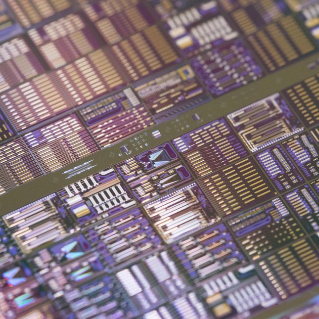
Photonic chips, powered by light rather than electricity, are the future. They will pave the way for self-driving vehicles, innovations in healthcare, and, of course, energy-efficient data and telecommunications. But bridging academic research to industry is not so straightforward. With this in mind, TU Eindhoven, University of Twente, TNO and PhotonDelta are launching the Photonic Integration Technology Center (PITC), a R&D center focused on accelerating the development of integrated photonics technology.
The possibilities of our current electronic chip technology are slowly but surely reaching their limits due to resistance, which is released in the form of heat as electrons travel through the copper conduits between transistors in chips. That resistance weakens the signal as it passes through the material.
Unlike electrons, light particles, or photons, lack mass and charge so they do not experience resistance. Moreover, light has properties allowing it to carry much more information, making it the ideal technique to accelerate the transfer of data within and between chips. Provided you know how to tame the light in the right way.
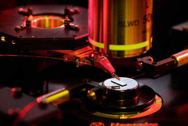
From lab to fab
TU/e has been putting significant investments into this lighting technology for years, and is a global leader in integrated photonic research. And while TU/e is well known for its close cooperation with industry, making the step from lab to factory could do with an extra push. Hence the new Photonic Integration Technology Center.

Sylwester Latkowski, TU/e researcher and the brand-new scientific director of the Center: "This R&D center will build a bridge to really get photonic chips to the market. In fact, we experience a gap when it comes to maturing the technology. As researchers, we work up to an advanced prototype, but the industry lacks the resources to move forward with that," Latkowski explains.
Knowing what the market needs
He continues: "Our role model is imec, the R&D hub for nano and digital technologies for semiconductor electronics industry. With them you really see how much value there is of having a large center for research and development in the chain. And that such an overarching center can perfectly well co-exist alongside the established institutes, start-ups, companies, large industries and universities."
Fortunately our work is not a matter of conjecture. Latkowski: "We know exactly what we need to do, what the next steps are and how we need to approach them. The bandwidth, the energy consumption, the price and the time frame.”
"In this respect, we also differ from academia. We're not targeting papers or mentoring PhD students. We are purely focused on what the industry is looking for, what the next generation products and applications need and at what moment which product is wanted," he explains.
This involves a very different scale than what researchers are used to. Latkowski: "Success is defined in a completely different way, and that requires a completely new way of thinking. What may be a large volume for academics and some of the businesses, say thousands of chips, is very small for industry. They measure success by seeing millions of chips a month rolling off the assembly line.”
Silicon or indium phosphide?
"Electronic chips and multiple forms of photonic chips will be used side by side over the next five to ten years," Latkowski predicts. The center is therefore fully committed to so-called hybridization, integrating a variety of photonic chips alongside electronic ones. As every material has its own strengths.
He refers to the various materials from which photonic chips can be constructed. A well-known material that TU/e researcher Kevin Williams and his group are working on, for example, is indium phosphide (InP), a material that can generate, modulate and amplify light itself but for which no very-large-scale infrastructure has yet been developed.
Silicon based chips can more easily be integrated with the current silicon based fabrication processes used for electronics. For example, the chips based on silicon nitride (Si3N4) that the University of Twente is developing or the full silicon chips that TU/e researcher Erik Bakkers and his group are working on, and which was recently demonstrated to be capable of emitting light”.
Self-driving car
That there is a market for cost-effective integrated photonic chips is apparent when we look at self-driving cars. Photonic components are already in use for the cameras and LIDAR modules that provide full surveillance of the surrounding and allow the vehicle to accelerate and brake automatically.
But one LIDAR sensor of an autonomous Google car, for example, can cost as much as 60.000 dollars. An autonomous car needs at least 6 of such sensors to be able to view the surroundings with sufficient extent of detail and not make any mistakes.
Latkowski: “The car industry has calculated that the photonic components should cost a maximum of 50 dollars to be a cost-effective solution for the car market. Integrated photonics can then be a game-changer. It brings many advantages over discrete component-based photonic systems, in terms of size, stability, performance, reliability, and cost.”
Full integration, in which one chip contains photonics and electronics together, is the next step. "Only then can photonics chips gradually take over as the costs of production become less and less," Latkowski concludes.
Media contact
Latest news

![[Translate to English:]](https://assets.w3.tue.nl/w/fileadmin/_processed_/e/0/csm_BvOF%202019_1031_BHF%20license%20TUe%20ILI%20copy_8a50884392.jpg "[Translate to English:]")