How pioneering a blueprint for chips made Eindhoven a leader in photonics
Photonic integration researchers Meint Smit and Weiming Yao talk about the challenges, the future and Eindhoven's success in photonics.
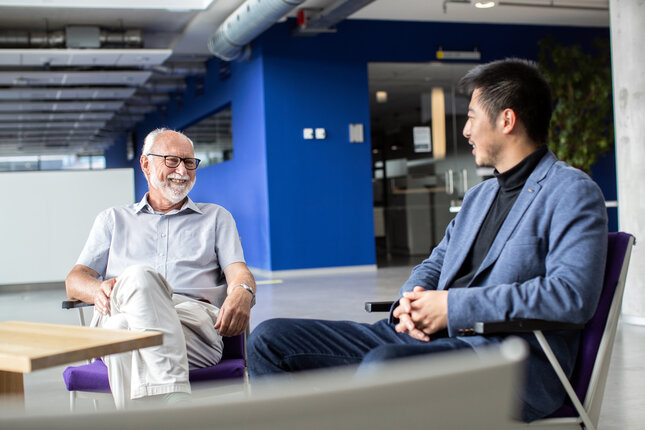
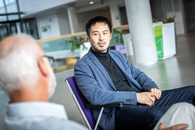
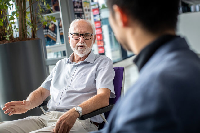
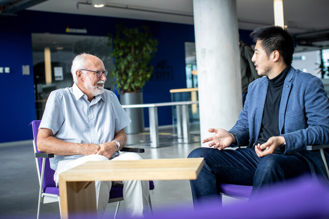
One has been pioneering for forty years and is considered among the founders of the photonic chip. The other, a pioneer of the present time, is at the forefront of innovation in photonics today. We brought them together, emeritus professor Meint Smit and young and up-and-coming talent Weiming Yao, for a conversation about the challenges in photonics then and now. About believing in your vision, competition among scientists and how everything always takes a factor pi more time than you think.
POWER TO THE PIONEERS
TU/e is celebrating its 65th anniversary, which is why in this lustrum year we are making a link between the past, the present and the future. In a series of double interviews we bring together pioneers from the past and present; pioneers who may have grown up in a different era, but who do share a common passion for a particular discipline. How do they view the (scientific) developments of then and now? What are the similarities and what are the differences? The earlier parts focused on sustainable mobility and robotics.
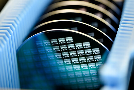
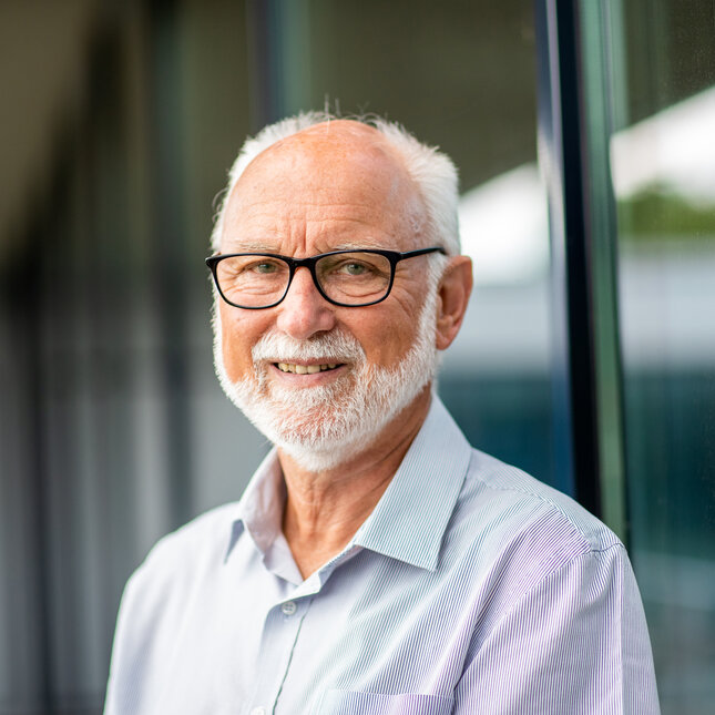
Probably without even realizing it, anyone reading this article has made use of an invention done by Meint Smit almost forty years ago. Officially, it's called an Arrayed Waveguide Grating (AWG): an optical component that plays an essential role in making a digital connection, whether online or a phone call.
Simply put, it allows light signals with different colors to be sent through a single fiber. "At one end it ‘combines’ the colors of light and at the receiver it separates them again so that the signals can be processed," Smit explains with restrained pride.
Thanks to this ‘color spectrum’, we can send dozens of times more information through a fiber, and nowadays many people in the world are using Smit's invention to communicate.
Visionary
It says enough about the influence he, until three years ago professor at TU/e and leader of the research group Photonic Integration, has had on the development of optical communication, or photonics. An icon in his field. A visionary too above all, who recognized early on that the route to success with photonic chips lay in the development of standard building blocks that could be used by anyone, developers, researchers or companies.
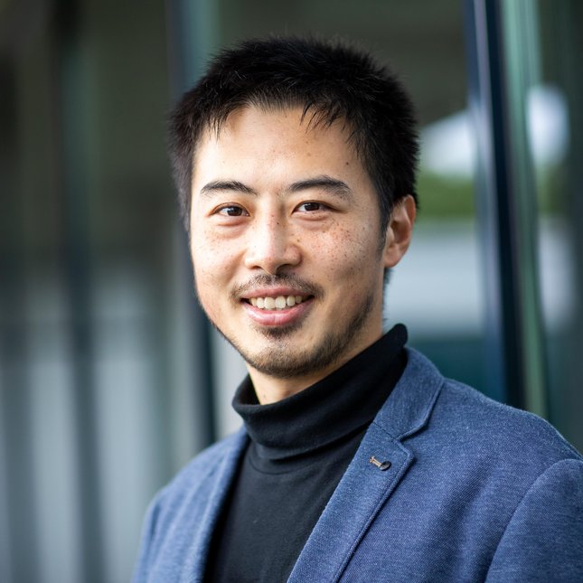
Weiming Yao is the pioneer of our time, you might say. Whereas Smit has been active in the field for almost forty years, the young assistant professor, originally from Germany, heard about optical communication for the first time, during his undergraduate studies in Berlin.
"I found it very exciting," says Yao. "I quickly realized that this was going to be a promising field with a lot of potential for the future and one I wanted to develop in." He would later join Smit's group (Smit: "It was immediately clear that he was a very clever guy.") and received his PhD four years later.
With a prestigious Veni grant, Yao is now exploring a new direction in the field of photonics, one that could not have been imagined years ago: artificial intelligence. His goal is to recreate artificial neural networks on a photonic chip.
Solving societal problems
So, photonic chips. Most people would never have heard of them until about ten years ago. But that is changing rapidly. "Photonics is causing a revolution similar to the one triggered by microelectronics in the 1970s," Smit thinks.
"Without photonics, the corona pandemic would have had a much larger negative impact on our society"
Two problems in today's data infrastructure make photonics a great promise: current microelectronics is running up against its limits; it can't get much smaller and faster. In addition, energy consumption must be drastically reduced if our information society continues to grow at such an exponential rate.
Communication with light has the advantage that it can transport much more information than communication with electrical signals, and with much less energy consumption.

For the record, photonics is already here. "A lot of people are probably unaware that photonics is integral to much of modern-day communication. Whether it's video streaming through 5G or because you're calling someone; the signals eventually go through optical glass fibers," says Yao.
And, adds Smit, photonics has proved its worth over the past year and a half. "Without photonics, the corona pandemic would have had a much larger negative impact on our society," he says. "We wouldn't have the capacity of the internet for all the necessary online communication."
The potential of optical chips is not limited to the worlds of data and telecommunication. Both researchers believe photonics can help solve societal challenges in numerous areas: from medical imaging to autonomous cars, and from smart material sensors in bridges and aircraft to the backbone of smart cities.
Neuromorphic
Yao believes photonic chips will additionally pop up in many more places you don't currently think of. "That was the case with electronic chips as well; we are now using them for applications we didn't know about ten years ago," he says. "A big advantage of a photonic chip is its potential for high speed and energy efficiency; that opens up numerous new doors."
His own research is a striking example. Yao focuses on ‘neuromorphic computing’, where computations are done with technology inspired by our own brains. "The challenge here is the huge computational power required and the speed at which you can do that," he explains.
Take the game Go, for which Google managed to train an algorithm that outperformed human players in 2016. Yao: "It took an enormous amount of time and energy to train this program on electronic hardware. I think that comparable tasks could be sped up and done more efficiently with photonic based neural networks in the future."
THe LAW Of pi
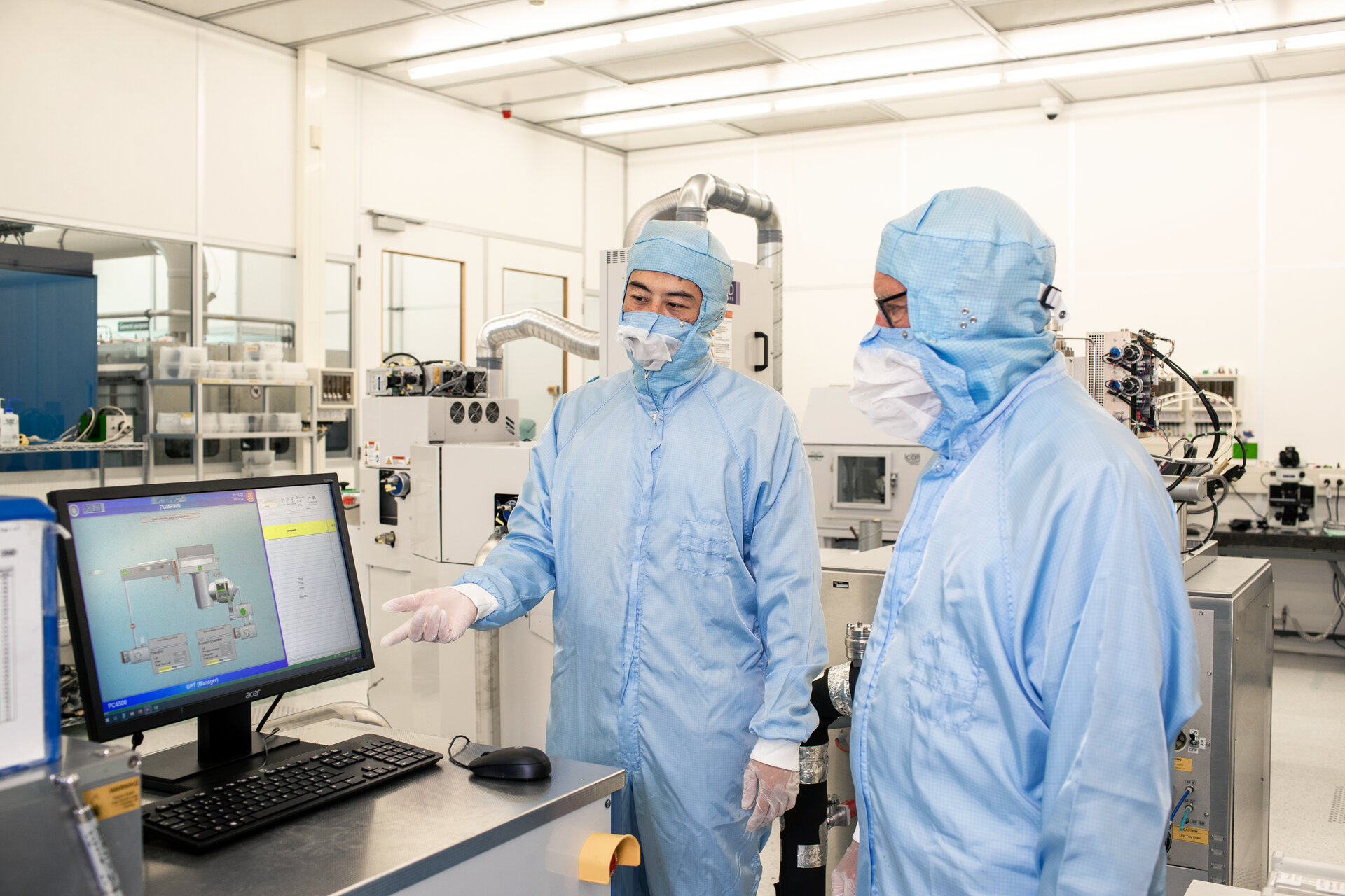
The Netherlands, and the Brainport region in particular, is world-leading in photonic chips. This is to large extent due to the work of Smit and his team. In the early 1980s, as an assistant in a new research group in Delft, he started pioneering in this promising field.
"The integration of photonics on a chip was a fairly new concept at the time; little was known about it," he recalls. "But because we saw that micro-electronics was starting to take off at that time, we believed that one day the same thing could happen with photonics."
"Something may seem easy to implement at first glance, but it always takes longer than you think"
Smit looks back on the 1980s as an exciting period. "It was creative. I had an idea which functions I wanted to realize, but how to do it was a challenge. There were few scientific papers to draw on. So you tried out all sorts of things yourself."
That's when he learned one of the most important lessons as a pioneer: you're always too optimistic. "Something may seem easy to implement at first glance," he chuckles, "but it always takes longer than you think."
"You tend to forget that if one of your machines breaks down you'll be delayed a few months. And if you need just those special screws that are out of stock you have another few months delay. Then when you finally succeed in making the machine, the first time it doesn't work and you spend a lot of time finding the cause of the problem. And sometimes you have the misfortune of having to start all over again."
Smit speaks of the law of pi: the time something actually takes is a factor of pi (about three) greater than the time you think it will take when you start. Do you think something can be realized in a year? It is more likely to take more than three years. Smit: "And that holds if you are experienced, for inexperienced people it is even pi squared, almost a factor of ten. That applied then, but it still applies now."
With some embarrassment, Yao confesses. "When I first started out in Eindhoven as a PhD student, it was indeed pi squared for me. It's mainly in the implementation. It’s very easy to overlook all the details that play a role. There is so much complex infrastructure needed to conduct research and every one of those components require good care. You don't usually think about that at the beginning."
And the law still applies. To give an example: Yao had hoped to realize his neuron on a chip within a year. "But we're already a year and a half in. Although we are really close now," he laughs.
Building the building blocks
Back to Smit's pioneering. After about ten years of component development, in the mid-1990s, his group was ready to start integrating a larger number of fundamental components on a chip. Getting that working took another ten years.
In that period – his group had moved to Eindhoven in the meantime – he gained an insight that would later prove crucial. For every new function they wanted to use the chip, they had to adapt the entire production process to optimize the technology. That's not going to work, he realized. For large-scale applications each of these processes takes years to get mature, which is ultimately going to cost tens of millions of euros per process.
He therefore chose a different route, that of standardization. "We wanted to arrive at a kind of basic process, which allows you to design and fabricate all kinds of different components, such as a sensor or a receiver," says Smit. So he started to develop a kind of library of 'basic building blocks', for which they knew in great detail how to make them. "We then combined these building blocks into new, more complex building blocks," Smit explains.
Step by step, Smit and his colleagues were able to work on optical chips with increasingly complex functions, including the surrounding infrastructure, such as measuring instruments and design software. Doing so, they created a standardized production process that was capable of realizing a large number of different functions with a limited number of building blocks.
Smit’s endeavours in Eindhoven met with some opposition, however. "People thought it would never work, that we would lose too much performance due to the compromises required to integrate all the building blocks in one single standardized process," Smit recalls. "And the physics community feared this approach would limit the freedom of design too much. Yes, we did sacrifice some of the freedom, but we felt that this sacrifice brought us a lot of new possibilities through the much larger complexity of photonic circuits that is possible in a mature and stable standardized process."
Smit persevered and, finally, after ten years of hard work, he was proven right. "In 2015 we were able to demonstrate that it really worked," he says proudly. Yao agrees. “It may have taken ten years to convince everyone, but by now most people accept that this is the way to go forward if you want to achieve complex integration. For example, you now also see large, industrial partners, who previously worked with specialized processes, moving to a foundry model."
Founding the foundry
A foundry. That is indeed what came into being in Eindhoven; a kind of public factory for the building blocks of photonic chips that others can use as a basis to build on, an important move on Smit's part. In this way, Eindhoven played a crucial role in laying the foundation for the new technology.
"With a click of a mouse a designer now conjures up a component with a complexity that we could only dream of twenty years ago”
"People could send in their designs and we combined a number of these designs on a single wafer," says Smit. With about ten academic and industrial partners, he founded the so-called JePPIX platform, in order to develop a foundry ecosystem. "The idea was to give universities and small companies access to expensive facilities they couldn't afford themselves," says Smit.
Yao, too, noticed what was going on in Eindhoven. “In 2011 I was doing my master's in Pisa, in Italy, and the group doing research on photonics there didn't have their own manufacturing process and facilities. So they sent their circuit designs to Eindhoven, where it was made into a chip and then sent back. I found that fascinating and realized then that one day I wanted to work in Eindhoven."
The accessibility of the technology accelerated development. Commercial companies were able to get started with practical applications of photonics. In 2012, the spinoff SMART Photonics was founded – originated from a cooperation of Smit's group with the former Philips Optoelectronics– for the industrial production of optical chips. Last year, the Dutch government put as much as 20 million euros into the young company.
"Nowadays, with the click of a mouse a designer can bring up a component with a complexity that we could only dream of twenty years ago and put it on a chip," Smit gloats. In the Brainport region, there is now a tight ecosystem in which companies, startups and knowledge institutes foster a strong 'collaborative spirit', experiences Yao.
Competition…
However, the pioneering is not finished yet. There are still major challenges for the field. The main one has to do with the fundamental material for the chip. Eindhoven and the partners within the JePPIX platform work with indium phosphide (InP). "A material with good properties that is excellent for optical components, such as lasers and modulators," says Smit.
"I expect the field to eventually move toward a situation where there is heterogeneous integration"
However, a competing material - silicon - has a larger constituency and, thanks to its large-scale infrastructure, better fabrication facilities. "The whole world has silicon plants," says Smit. “That technology has more advanced equipment. We use equipment in our clean room that was developed for silicon thirty years ago."
But: silicon has the disadvantage that it is actually not very suitable for working with light, it does not support the most important optical components: lasers and optical amplifiers. Smit: "The problem is simple: we have a superior material but the wafers are smaller and the technology is less developed."
The competition has been going on for over twenty years now, during which Smit experienced that the silicon community was strongly dominating the publicity about photonic integration. "They strongly believed that silicon had the future, and were quite active in promoting that belief." It made Smit, for example, struggle to get funding because some reviewers of his proposals also doubted InP.
... and collaboration
It is precisely because of this competition that there is very close cooperation within the InP field, Yao observes. "There is little point in inventing things in parallel. It works much better to join forces and that you can use each other's technology."
What is the endgame here? "There will be applications for indium phosphide alone and also for silicon alone, but one of the biggest challenges for the coming time is to bring photonics and electronics together on the same chip," Smit predicts. "Silicon and indium phosphide will eventually integrate in this process."
Yao also thinks the two materials are on track to meet each other. "People in silicon photonics are increasingly realizing that they also need other materials, because you can't make all the applications with silicon alone. I expect the field to eventually move toward a situation where there is 'heterogeneous integration': different material platforms linked together."
And that's what Smit and his colleagues are already working on, with, for example, a thin membrane of indium phosphide on top of a layer of silicon. Earlier this year, the TU/e, together with UT and TNO, launched a new R&D center called Photonic Integration Technology Center to give the step from lab to fab an extra push. Smit: "There is still a long way to go, it’s far from commercial."
In short, let's not rejoice too soon, bearing in mind the law of pi. But we can safely trust Smit that the revolution will come, eventually.
The latest news