Cracking and Tracking of Quantum Dot Formation
Raja Gajjela defended his PhD thesis at the department of Applied Physics on November 11th.

The Quantum revolution is the next big step for humanity as it will have a great impact on multiple fields of science and technology such as chemistry, medicine, computing, electronics, etc. Researchers across the globe are competing to develop new technologies and highly efficient electronic devices. Quantum dots (QDs) are three-dimensional islands with nanometer dimensions that combine the best of semiconducting materials and quantum mechanical effects to improve the efficiency of devices such as lasers, QLED displays, solar cells, flash memories, etc. QDs are also considered potential candidates for qubits for quantum computing and quantum information technologies. All the above-mentioned applications strongly depend on the QDs' size, shape, and composition. Therefore, it is essential to understand how these QDs are formed at the atomic level if one wants to exploit their full potential. For his PhD research, Raja Gajjela investigated the size, shape, and composition of different semiconductor QDs and answered important questions regarding the growth.

Scanning tunneling microscopy
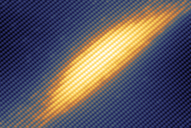
It is impossible to see these QDs with a naked eye, they are so small that we need complex microscopic equipment to analyze them. Thanks to the major developments in the field of microscopy many such techniques are available today. One of those techniques is scanning tunneling microscopy (STM) which works on the principle of quantum mechanical tunneling. In STM, a sharp metallic tip is brought close to the surface when the distance is very small, the electrons start to flow from the sample to tip or tip to sample even though there is a gap between them. The resolution of STM is so high that one can actually see the atoms as shown in the image.
Growth of QDs
In his PhD thesis, Gajjela used a cross-sectional STM to study the size, shape, and composition of different semiconductor QDs for different applications such as InAs/InP QDs for quantum information technologies, (In,Ga)(As,Sb)/GaP QDs for flash memories, InAs/GaAs submonolayer QDs for infrared photodetectors, etc. Thanks to the uniqueness of cross-sectional STM, we are able to answer important questions regarding the growth of QDs and provided direct and detailed feedback to further improve QDs-based electronic and optoelectronic devices. The results obtained in this thesis have been published in five articles in leading international journals with open access to anyone.
This thesis is a result of excellent collaboration between Toshiba Europe Limited in Cambridge, the University of Sheffield, the Oxford University in the U.K, the Technical University of Berlin, the University of São Paulo in Brazil, and the Eindhoven University of Technology as a part of collaborative European Innovative Training Network (ITN) funded by the Marie Sklodowska-Curie Actions (MSCA) in Horizon 2020, under the project name 4PHOTON.
Title of PhD thesis: Cracking and Tracking of Quantum Dot Formation
Supervisors: Paul Koenraad, Stefano Sanguinetti (external)