Sub-nanometer metrology for SEMICON High Volume Manufacturing
NOMI Nearfield report by Anton van Dijsseldonk, TU/e HTSC, and Rob Willekers, TNO.
The further development of microchips/semiconductor devices is necessary to enable sustainable, energy-saving solutions for future challenges in the computing needs of deep learning, Internet of Things, medical applications, Artificial Intelligence, etc. The semiconductor industry is continuing its pace in driving (or following) Moore’s law and thus keeps doubling the number of transistors per cm2 about every two years. This is done by reducing the smallest features that can be printed on a wafer using the latest technologies in lithographic equipment. However, the physics of semiconductor devices (and thereby the layout) also need to be adapted in order to be able to make reliable Integrated Circuit (IC) devices at ever smaller device structure dimensions.
Smaller nodes
Today, the High Volume Manufacturing (HVM) of leading edge ICs is around the 7 nm node, and the fin field-effect transistor (FinFET) is the mainstream device structure in logic devices. As can be seen in the figure below (from Applied Materials), the device structure (or transistor structure) will need to change quite dramatically when going to the smaller nodes.
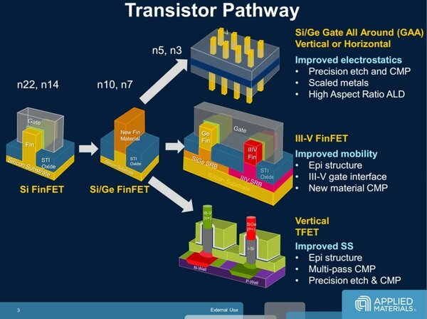
It is also obvious from the figure above that at smaller nodes, device architectures are becoming increasingly complex through 3D integration, new materials, new and additional manufacturing technologies, etc. All this increased complexity is required while tolerances on dimensions, placement and dopant levels are narrowed. The International Roadmap for Devices and Systems (IRDS) expects Gate All Around FETs to become a major player in the 3 nm node era, with GAAFETs replacing FinFETs at the 2 nm node.
This need for continued shrinking and efficiency in semiconductor devices has to be supported by the appropriate metrology methods for the high-volume manufacturing of microchips for the 3 nm node and beyond. Innovative breakthroughs are needed to enable quantitative metrology in three dimensions at the sub-nm scale. References can be found in the IRDS and industry roadmaps. This new metrology method is a crucial step in enabling the HTSM SEMICON equipment roadmap for 3D profiling equipment.
One thus requires a system that can make observations at the nanoscale or, more precisely, that can accurately make measurements in all three dimensions with the appropriate accuracy and precision at that scale. Such a system is, by nature, multidisciplinary as an ultra-precise mechanical system needs to be combined with an optical system, an electronics system, a control system, etc. The development of such a system matches perfectly with the Nano Opto-Mechatronics Instruments (NOMI) collaboration of TU Eindhoven’s High Tech Systems Center (HTSC) and TNO.
Nano Opto-Mechatronics Instruments (NOMI) collaboration
NOMI was set up to drive technology innovations for the development of instruments to image, measure and fabricate devices at sub-nm scales. It has started a project with industrial partner Nearfield Instruments to provide the fundamental breakthroughs needed to enable (sub-)nm scale metrology for semiconductor HVM at the 2 nm node and beyond. This is obviously in line with both the semiconductor roadmap and the semiconductor equipment roadmap. The equipment roadmap details the requirements for all equipment, including metrology equipment, which is required for the cost-effective (high-volume) manufacturing of ICs at these small scales.
What is the expected outcome of the project? One of the concrete goals is the theoretical modelling of 3D metrology using Nearfield Instruments technology; other goals are the development of a measurement platform and improvements to the control strategy. All of the above will enable a next major step in quantitative 3D metrology. Clear deliverables have thus been defined for i) modeling, ii) simulation and iii) control and technology demonstrator development for probe-based profiling.
The four-year project is now about to start (September 2020) and will enable and support the training of two PhD students and one PDEng student, but is expected to leverage more in the future in terms of both education and technology development. The results of the project will be used by Dutch OEMs to further develop metrology equipment for 3D metrology fit-for-purpose in the semiconductor industry.
In a future article, we will report more details together with Nearfield Instruments.