Researcher in the Spotlight: Sven Sperling
understanding of wear mechanisms and wear particle formation on silicon wafers in lithography modules
Hi, my name is Sven Sperling and I work in the Mechanics of Materials research group of the Department of Mechanical Engineering. My research is concerned with the numerical simulation of silicon wafer wear particle detachment due to machine contact in lithography modules.
Wear and tear on the nanoscale
These days, the projection resolution in lithography modules reaches 10 nm. The projection of these fine patterns is essential in the manufacturing process of small-scale electronic products, for which silicon wafers serve as a base material.
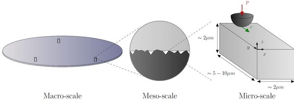
Contact between machine parts and the silicon wafer initiates a wear-like mechanism that interferes with this projection in two ways: (i) damage accumulates at the bottom of the wafer, causing it to tilt on the stage, and (ii) wear particles which have detached from the surface may interfere with the EUV light.
To better understand the mechanics of wear particle formation, a computational model will be established. The computational routine will be derived from a micro-scale single asperity model in accordance with the large-scale contact situation. With this model, we can engage in predictive modeling and investigate the parameters with prominent role in the detachment of wear particles.
Pushing computational boundaries
A strong simulation tool for structural mechanics problems is the Finite Element Method (FEM). However, this is less convenient when complex fractures dominate the material response due to being based on continuum assumptions. A second tool is Molecular Dynamics (MD) in which individual atoms are modeled according to an atomic interaction potential. This preserves the discrete structure of materials and is thus more suitable for complex fractures. Nevertheless, microscale simulations require a drastic number of individual atoms and therefore push computational resource boundaries.
The second challenge is evaluating a proper constitutive model which describes the silicon material at the microscale. While silicon is brittle at the macroscale, micro and nanoscale indentation tests have proven that silicon suffers from pressure-induced phase transitions. These phase transitions are important for two reasons: they cause the material properties to change (e.g., lower stiffness) and introduce a residual stress field that may govern crack propagation and initiation beneath the surface.
A new particle method approach
After a broad investigation of computational methods, we have concluded that existing particle methods are insufficient due to compromises regarding proper continuum behavior. We have therefore started to develop a continuum-consistent particle method which can include arbitrary fracture paths in a deformable body. We are currently conducting simulations that illustrate the constitutive flexibility of the method by comparing it with FEM and other particle method simulations.
"As a result, we can unravel the mechanics involved in the detachment of wear particles"
My computational model will contribute to our understanding of wear mechanisms and wear particle formation on silicon wafers in lithography modules. This will allow us to study the influence of individual parameters (such as indentation size, speed and shape) on the mechanical response in the material. As a result, we can unravel the mechanics involved in the detachment of wear particles by investigating parameters that are extremely difficult to measure. This can inspire design guidelines to maintain or even decrease small projection resolutions in lithography modules, thereby pushing the boundaries of semiconductor manufacturing and resulting in more efficient and compact electronic products.