Manipulating light at the atomic scale
With a START-UP grant worth 600.000 euros from NWO, PSN-researcher Alberto Curto wants to open up a whole new field of research in the next four years. ‘We want to push the limits of photonics by realizing active control of light in one monolayer of material.’
Curto got the grant in the first round of a new NWO scheme, intended for recently appointed assistant and associate professors in physics and chemistry to develop creative, risky ideas that lay the foundation for the research themes of the future or bring about scientific innovations. In his office, he takes us through his research plans and ambitions.
What is your START-UP project about?
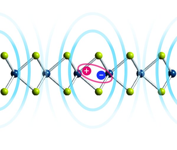
‘In this project, we will pursue the ultimate limit of light control: the atomic scale. Layered 2D semiconductors can be used as nearly ideal sources and detectors for nanophotonics. They exhibit a strong optical response and give access to exciting electronic degrees of freedom like the spin, valley and layer indexes. By making use of the extreme light-matter interaction that is enabled by monolayer 2D semiconductors, we aim to demonstrate guiding of optical waves bound to atomically thin materials. These waves then can open the gate to active control of nanoscale light in tunable devices.’
How are you going to do this?
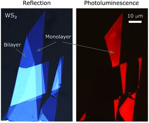
‘We are going to employ a combination of optical microscopy and spectroscopy, light emission and photodetection techniques, nanofabrication, and nanophotonic simulations. This project merges concepts and techniques from nano-optics with the physics of ultrathin semiconducting materials. We are focusing on two-dimensional semiconductors with graphene-like structures. What makes these structures special is that they have a direct bandgap in the visible part of the spectrum, that only opens up when you peel down the material to one monolayer of thickness. Thus, a monolayer of the material enables bright light emission, whereas a piece of the same material that is several layers thick is dark. We are going to explore if it is possible to scale down optics to one atomic layer to achieve active tunable devices.’
What is the main challenge here?
‘We need to identify semiconductors that interact strongly enough with light, even when thinned down to a single atomic monolayer. Guiding and confining light using such ultrathin films requires extreme material properties.
In monolayers of transition metal dichalcogenides (TMDs), such as WS2, absorption can reach 16 percent at a wavelength of 605 nanometers, in a layer that is only 0.7 nanometer thick. Bounding a propagating optical wave to such a material is our first aim.’
What makes this field of research so exciting?
‘Where you would normally use plasmons - collective oscillations of the free electron gas density - or free carriers in the metal, we now will now use the response of the material itself to guide the light. To be able to do this, phenomena like dispersion, confinement and decay during propagation are of vital importance, as is the change in refractive index of the different material layers.
This field of research can enable a whole new platform of devices, such as modulators, photodetectors and so on. Imagine for example a sensor that can measure changes in the refractive index, that could be used to detect molecules in solutions in a very sensitive way.’
‘We are also going to combine optics with more electronic degrees of freedom, for example addressing the spins of electrons with the polarization of light. The use of light to manage the flow of the electrical carriers in the material could lead to a new type of functionality, for which the word valleytronicshas been coined.’
You obtained your PhD in Photonics at ICFO - The Institute of Photonic Sciences in Barcelona - and did a subsequent postdoc as a Marie Curie fellow at Stanford University. Why did you decide to come to TU/e?
‘TU/e is well known for photonics research. Here both physicists and engineers work with light at the Institute for Photonic Integration, which means that we can achieve more together. Eindhoven also provides the right industrial environment to make my research reach potential users. Furthermore, the infrastructure here enables researchers to fabricate the necessary structures for total control over light at the nanoscale.’
What is your ultimate dream?
‘This project explores a niche area that combines 2D semiconductors with nano-optics, and the emerging properties from the interface between them. I hope to demonstrate the operation of a device that can guide light waves, and subsequently demonstrate tunability.’
‘Furthermore I hope to identify materials that operate at different wavelengths. Currently we work in the visible domain between 600 and 800 nanometers. But if we can find materials that exhibit the same behavior at, for example, infrared wavelengths, they would be very interesting for photonic integration applications.’
Alberto Curto is looking for researchers who want to work with him on this project. He currently has a vacancy for a PhDand for a postdocposition. Talented people with experience in relevant fields are more than welcome to contact him for further information.
Read the news article about the granted START-UP grants here
Cursor wrote a short story on the grants, which can be read here
More information about Alberto and his research can be found here