Ultracold ion beams
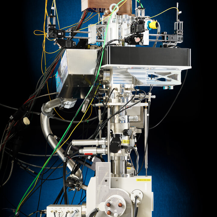
Focused Ion Beam (FIB) instruments are important tools for the semiconductor industry. Essential applications are editing circuits and repairing masks in the development phase, failure analysis during wafer processing, and preparing samples for inspection using transmission electron microscopy. As a result of the continuing reduction of feature sizes in semiconductor circuits, FIBs also face higher demands, in particular in terms of resolution and reduced damage. We have developed a unique, proof-of-principle FIB instrument that overcomes the limitations of existing FIBs. The essential innovation is the use of a new type of ion source that is based on photo-ionization of a laser-intensified and extremely cold atomic rubidium beam. In this project, the properties of the new instrument are assessed and optimized with the eventual aim of creating a practically useful prototype instrument that allows for 1 nm resolution in imaging and milling.
Focused Ion Beam (FIB) instruments are important tools for the semiconductor industry. Essential applications are editing circuits and repairing masks in the development phase, failure analysis during wafer processing, and preparing samples for inspection using transmission electron microscopy. As a result of the continuing reduction of feature sizes in semiconductor circuits, FIBs also face higher demands, in particular in terms of resolution and reduced damage. We have developed a unique, proof-of-principle FIB instrument that overcomes the limitations of existing FIBs. The essential innovation is the use of a new type of ion source that is based on photo-ionization of a laser-intensified and extremely cold atomic rubidium beam. In this project, the properties of the new instrument are assessed and optimized with the eventual aim of creating a practically useful prototype instrument that allows for 1 nm resolution in imaging and milling.