Nanofabrication & Thin-Film Engineering
At FNA we investigate the intricate physics of nanostructured devices made of thin-films and 3D structures. The deposition and patterning of complex multilayered ultrathin (<1 nm) films allows us to address many physical phenomena. The thin films are produced in our dedicated UHV sputter and evaporation chambers and the nanofabrication takes place at NanoLab@TU/e, a state-of-the-art cleanroom, where UV photolithography, E-beam lithography and various etch and milling techniques can be used for pattern transfer. By designing and engineering smart structures the intricate physics that occurs at interfaces between (magnetic) metals, insulators and semiconductors are investigated.
NanoLab@TU/e
In NanoLab@TU/e all equipment for pattern definition is available, ranging from UV to electron beam lithography, chemical benches for wet etching and plasma tools for dry etching. Further characterization tools include scanning electron microscopy, focused ion beam etching, focused electron and ion beam induced deposition and XRD, depth-profiling XPS etc.
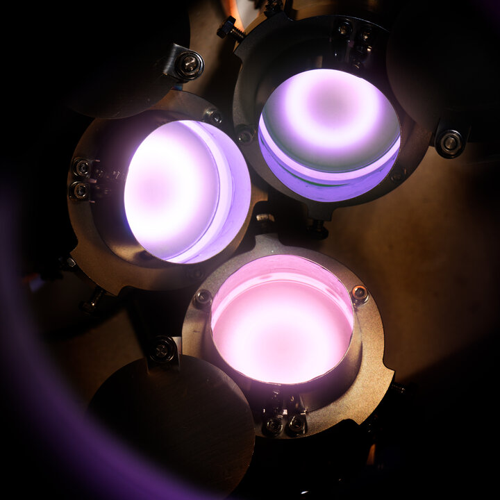
Nanofilm@FNA
In our UHV nanofilm lab we can deposit different materials layer by layer using DC, RF, reactive and pulsed magnetron sputtering and evaporation. Typically ultrathin multilayers are made which allows us to address the intricate physics that happens at the interfaces.
At FNA we investigate the intricate physics of nanostructured devices made of thin-films and 3D structures. The deposition and patterning of complex multilayered ultrathin (<1 nm) films allows us to address many physical phenomena. The thin films are produced in our dedicated UHV sputter and evaporation chambers and the nanofabrication takes place at NanoLab@TU/e, a state-of-the-art cleanroom, where UV photolithography, E-beam lithography and various etch and milling techniques can be used for pattern transfer. By designing and engineering smart structures the intricate physics that occurs at interfaces between (magnetic) metals, insulators and semiconductors are investigated.
NanoLab@TU/e
In NanoLab@TU/e all equipment for pattern definition is available, ranging from UV to electron beam lithography, chemical benches for wet etching and plasma tools for dry etching. Further characterization tools include scanning electron microscopy, focused ion beam etching, focused electron and ion beam induced deposition and XRD, depth-profiling XPS etc.
Nanofilm@FNA
In our UHV nanofilm lab we can deposit different materials layer by layer using DC, RF, reactive and pulsed magnetron sputtering and evaporation. Typically ultrathin multilayers are made which allows us to address the intricate physics that happens at the interfaces.