Atomic scale processing
We aim to develop advanced atomic layer deposition and etching processes through in-depth understanding of the underlying reaction mechanisms. With this we try to enable future device technologies in nanoelectronics, photonics, photovoltaics and beyond.
Atomic scale processing for future device technologies
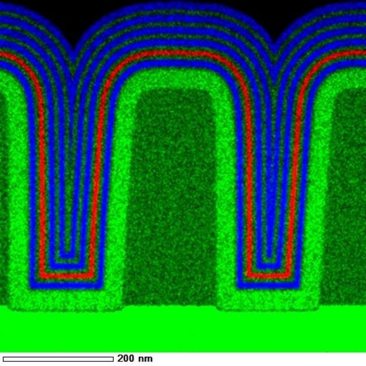
Whether it is in the field of nanoelectronics, photonics, photovoltaics or quantum technology, future device technologies will heavily depend on atomic scale processing techniques such as atomic layer deposition (ALD) and atomic layer etching (ALE). These techniques allow for atomic-scale control and they provide many opportunities for bottom-up processing of the multitude of materials that will make up future devices. With our research we try to develop advanced processes that will enable these future device technologies. Current interests include thermal and plasma-assisted ALD and ALE processes as well as area- and topographically-selective processing. Very importantly, it also involves fundamental studies of the underlying reaction mechanisms through advanced in situ studies coupled to atomistic modelling. Our direct research partners are mostly equipment manufacturers and suppliers of chemicals.
News


Recent Publications
Our most recent peer reviewed publications
-
Willem-Jan H. Berghuis,Marvin A.J. van Tilburg,W.H.J. Peeters,V.T. van Lange,Riccardo Farina,Elham Fadaly,R.J. Theeuwes,Marcel A. Verheijen,Bart Macco,Erik P.A.M. Bakkers
Low Surface Recombination in Hexagonal SiGe Alloy Nanowires
ACS Applied Nano Materials (2024) -
Emanuele Bochicchio,Ksenia Korzun,Bas T. van Gorkom,Roel J. Theeuwes,Wilhelmus M.M. Erwin Kessels,Jaime Gómez Rivas,Jos E.M. Haverkort
Optimization of the efficiency of a nanowire solar cell by nanowire tapering
Journal of Applied Physics (2023) -
Mike van de Poll,Hardik Jain,James N. Hilfiker,Mikko Utriainen,Paul W.G. Poodt,W.M.M. Kessels,Bart Macco
Excellent conformality of atmospheric-pressure plasma-enhanced spatial atomic layer deposition with subsecond plasma exposure times
Applied Physics Letters (2023) -
Nga Phung,Dong Zhang,Cristian A.A. van Helvoirt,Michael Verhage,Marcel A. Verheijen,V. Zardetto,Frennie Bens,Christ H.L. Weijtens,Bart L.J. Geerligs,W.M.M. Kessels
Atomic layer deposition of NiO applied in a monolithic perovskite/PERC tandem cell
Solar Energy Materials and Solar Cells (2023) -
Silke A. Peeters,Ciaran T. Lennon,Marc J.M. Merkx,Robert H. Hadfield,W.M.M. Kessels,Marcel A. Verheijen,Harm C.M. Knoops
Ultrathin superconducting TaCxN1-x films prepared by plasma-enhanced atomic layer deposition with ion-energy control
Applied Physics Letters (2023)