Advanced ALD technologies
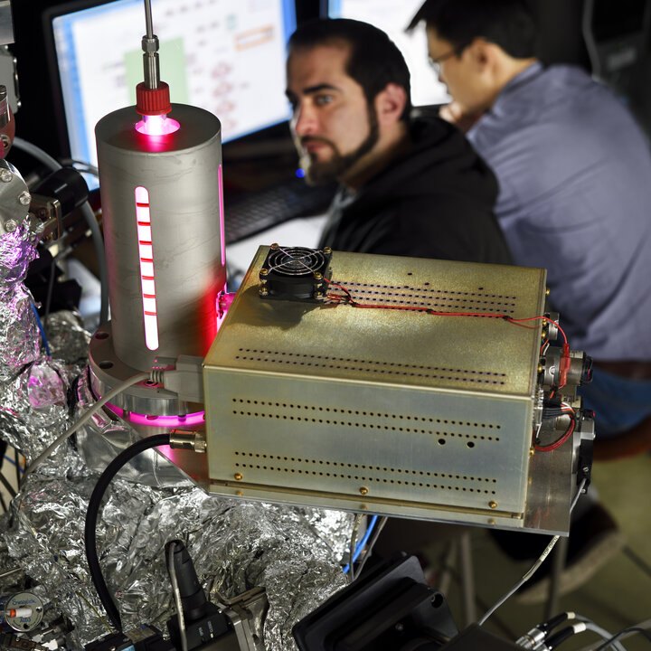

In the Plasma & Materials Processing (PMP) group we have a consolidated expertise in ultrathin film growth by means of ALD. ALD is based on the alternating dosing of precursors and co-reactant gases separated by purge or pump steps. The thin films are grown in a layer-by-layer fashion due to the limited amount of precursor or gas that reacts with the substrate surface in each dose step. ALD therefore allows for sub-nanometer thickness control, excellent uniformity and superior step coverage. By investigating advanced ALD cycles for enhanced material properties, by adding extra reactivity to the ALD process with a plasma for low temperature processing, and by developing area-selective ALD for nanopatterning, we work on cutting-edge process technologies that are relevant for advancing the (industrial) application of ALD.Advanced ALD cycles We explore the potential of ALD processes by expanding the regular two-step cycle approach to the multi-step approach and the supercycle approach. This enables the deposition of advanced materials (i.e. binary and ternary oxides) and also further tuning of film properties. For example, in the deposition of Pt thin films at low temperature with a Me3(MeCp)Pt exposure step and an O2 plasma, PtOx is usually obtained. In our group we introduced a third step, consisting of an H2 plasma, in order to reduce PtOx to Pt. With the 'supercycle' approach multiple ALD processes can be combined for doping of thin film (e.g. Al-doped ZnO) or prepare multi-component compounds (e.g. SrTiO3).Plasma-assisted ALDPlasma-assisted ALD is an energy-enhanced ALD method that is rapidly gaining in popularity. Because of the high reactivity associated to the plasma species, less thermal energy is required at the substrate to drive the ALD surface chemistry. Amongst others, this opens opportunities to synthesize films at lower substrate temperatures than for thermal ALD. Low temperature-ALD is particularly advantageous for deposition on temperature-sensitive substrates. We investigate for example ALD of SiNx and Al2O3 below 100°C for the application as moisture barrier layers for flexible organic electronics. Another process developed in our group involves the low temperature deposition of ultrathin films and nanoparticles of Pt. Deposition of Pt on materials, such as polymers, fabrics and fibers paves the way to applications such as flexible electronics, thin film solar cells and catalysis.
Area-selective ALD
The conventional way to pattern ALD films in the semiconductor industry is by lithography. Apart from the subtractive method using etching, it is also possible to block a part of the surface with photoresist before doing ALD. This method, that is called lift-off lithography, is a so-called area-deactivation method of area-selective ALD. Within PMP, we have developed a method for area-selective ALD by locally activating regions at the surface. Since ALD depends critically on surface chemistry, it is possible to chemically modify the surface for locally stimulating growth while preventing growth at other regions. The chemical modification can for example be done with a patterned seed layer that catalyzes the surface reactions of the selected ALD process. For the area-selective deposition of Pt, first a seed layer is deposited in a pattern predefined by electron beam induced deposition (EBID). Then in the Pt ALD process, the surface is alternately exposed to MeCpPtMe3 precursor and O2 gas at a substrate temperature of 300 °C. The ALD growth on the seed layer pattern is locally promoted and the pattern is built bottom-up in thickness during the ALD processing. Moreover, contaminants in the seed layer pattern prepared by EBID are removed during ALD, resulting in pure Pt structures. This method enables the nano-patterning of high-quality material with a lateral resolution of only 10 nm. The combination of EBID and ALD, referred to as direct-write ALD, is therefore a viable alternative to lithography-based patterning with a better compatibility with sensitive substrates, as for example used in future nanoelectronics.