Interfaces in future energy technologies
Presently, novel ALD merits are unraveled when atomic layer processing meets energy conversion and storage technologies such as photovoltaics, batteries and (electro-)catalysis. Growth control on physically challenging substrates (e.g. 1D and 2D materials, porous scaffolds, and powders) and material synthesis ranging from nanoparticle to continuous films are tangible examples. Our contribution to this exciting research area is the design and engineering of atomic scale processed interfaces and thin films, which are key to promotion of selective charge carrier transport in energy devices, such as metal halide perovskite solar cells, tandem solar cells, (Li-ion) batteries and (electro-)catalysis.
Interface engineering for next generation energy technologies
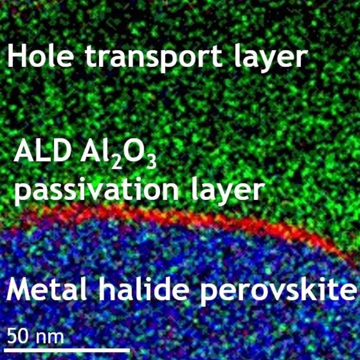
Our approach is multidisciplinary, as it embraces material science and solid-state physics, together with the integration of atomically grown thin films and interfaces in devices. Moreover, the design and engineering of interfaces for future energy technologies require atomic scale processing to go beyond its state-of-the art. This is the case of ALD processing on 'chemically challenging substrates', such as metal halide perovskite absorbers for single and tandem photovoltaics devices. This application field demands advancement in the level of control in ALD growth to avoid modification of the perovskite surface and bulk chemistry. Scientifically, we pursue this goal by gaining insights, with the aid of in situ diagnostics, into the ALD surface reactions and film growth mechanisms on perovskite. Another exciting example is the field of (electro-)catalysis. When 'borrowing' from ALD the principle of digital design of materials, we can synthesize electro-catalysts with atomic precision in terms of morphology, chemical composition and size and distribution of (nano-)particles.
News


Contact
Meet some of our Researchers
Recent Publications
Our most recent peer reviewed publications
-
Dirk Jonker,Cavit Eyovge,Erwin Berenschot,Valerio Di Palma,Dorothee Wasserberg,Sandra Michel-Souzy,Pascal Jonkheijm,Silke Krol,Han Gardeniers,Mariadriana Creatore
Electrochemical Sensing with Spatially Patterned Pt Octahedra Electrodes
Advanced Materials Technologies (2024) -
Wiria Soltanpoor,Andrea E.A. Bracesco,Nathan Rodkey,Mariadriana Creatore,Monica Morales-Masis
Low Damage Scalable Pulsed Laser Deposition of SnO2 for p–i–n Perovskite Solar Cells
Solar RRL (2023) -
Sina Haghverdi Khamene,Cristian A.A. van Helvoirt,M. Tsampas,M. Creatore
Electrochemical Activation of Atomic-Layer-Deposited Nickel Oxide for Water Oxidation
Journal of Physical Chemistry C (2023) -
Xin Zhang,Andrea Bracesco,Wenya Song,Stijn Lenaers,Wouter T.M. van Gompel,Anurag Krishna,Tom Aernouts,Laurence Lutsen,Dirk J.M. Vanderzande,M. Creatore
Surface Modulation via Conjugated Bithiophene Ammonium Salt for Efficient Inverted Perovskite Solar Cells
ACS Applied Materials & Interfaces (2023) -
Nga Phung,Dong Zhang,Cristian A.A. van Helvoirt,Michael Verhage,Marcel A. Verheijen,V. Zardetto,Frennie Bens,Christ H.L. Weijtens,Bart L.J. Geerligs,W.M.M. Kessels
Atomic layer deposition of NiO applied in a monolithic perovskite/PERC tandem cell
Solar Energy Materials and Solar Cells (2023)