Processing of low-dimensional nanomaterials
Driven by Moore’s scaling law and the transition to a sustainable society there is an enormous push to develop nanomaterials for novel device architectures and for device concepts with new functionalities. In order to study new nanomaterials systematically and later implement them into devices, new synthesis processes and techniques need to be investigated and developed, that are reliable, reproducible and scalable with ultimate control at the nanoscale.
Synthesis and integration of 2-D nanomaterials
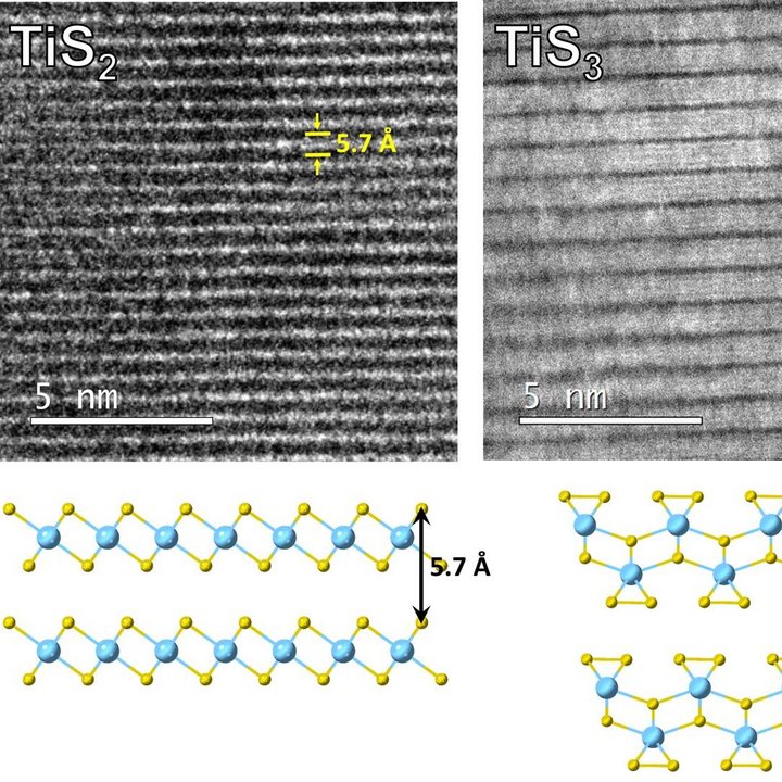
In our group we pioneer atomic layer deposition (ALD) for 2D nanomaterials synthesis. ALD is a scalable, low temperature preparation method for thin films which offers precise thickness control down to the sub-monolayer and can therefore be instrumental for the large area synthesis of 2D materials. The current focus of the group is on ALD of 2D transition metal dichalcogenides (2D-TMDs) for (opto)electronics and catalysis. We use plasma chemistry (plasma-enhanced ALD, PEALD) to control functionalities of the 2D-TMDs, such as morphology, materials phase and stoichiometry. Furthermore, by doping, alloying and by the formation of heterostructures we tune the electrical properties of the 2D TMDs, such as the charge carrier concentration and band gap.
Read more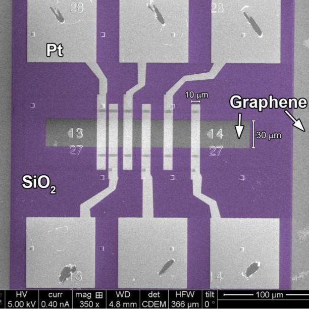
Integration of 2-D nanomaterials
Another challenge in the 2D nanomaterials field is how to connect these materials efficiently to the outside world. For example, properly functioning contacts and dielectrics need to be fabricated on top of the 2D materials to make functioning nanodevices. Furthermore, patterning of the new nanomaterials also brings in new integration challenges. Patterning of 2D materials conventionally involves lithography using resist films. However, resist residues deteriorate the nanomaterials properties.
In our group we develop new techniques to contact and pattern the 2D nanomaterials. For example, we investigated new techniques based on ALD to form metals and dielectrics on top of graphene, without deteriorating its properties. In addition, to avoid contamination by resist residues as much as possible, we developed a direct patterning approach using a focused ion beam to pattern graphene. Besides we developed new processes for selective area deposition of metals and 2D TMDs for device applications.
Contact
Meet some of our Researchers
Recent Publications
Our most recent peer reviewed publications
-
Willem-Jan H. Berghuis,Marvin A.J. van Tilburg,W.H.J. Peeters,V.T. van Lange,Riccardo Farina,Elham Fadaly,R.J. Theeuwes,Marcel A. Verheijen,Bart Macco,Erik P.A.M. Bakkers
Low Surface Recombination in Hexagonal SiGe Alloy Nanowires
ACS Applied Nano Materials (2024) -
Emanuele Bochicchio,Ksenia Korzun,Bas T. van Gorkom,Roel J. Theeuwes,Wilhelmus M.M. Erwin Kessels,Jaime Gómez Rivas,Jos E.M. Haverkort
Optimization of the efficiency of a nanowire solar cell by nanowire tapering
Journal of Applied Physics (2023) -
Mike van de Poll,Hardik Jain,James N. Hilfiker,Mikko Utriainen,Paul W.G. Poodt,W.M.M. Kessels,Bart Macco
Excellent conformality of atmospheric-pressure plasma-enhanced spatial atomic layer deposition with subsecond plasma exposure times
Applied Physics Letters (2023) -
Nga Phung,Dong Zhang,Cristian A.A. van Helvoirt,Michael Verhage,Marcel A. Verheijen,V. Zardetto,Frennie Bens,Christ H.L. Weijtens,Bart L.J. Geerligs,W.M.M. Kessels
Atomic layer deposition of NiO applied in a monolithic perovskite/PERC tandem cell
Solar Energy Materials and Solar Cells (2023) -
Silke A. Peeters,Ciaran T. Lennon,Marc J.M. Merkx,Robert H. Hadfield,W.M.M. Kessels,Marcel A. Verheijen,Harm C.M. Knoops
Ultrathin superconducting TaCxN1-x films prepared by plasma-enhanced atomic layer deposition with ion-energy control
Applied Physics Letters (2023)