Processing of nanomaterials
One of the research areas with the Plasma & Materials Processing (PMP) group is to study the growth and synthesis of 0D, 1D and 2D nanomaterials such as nanoparticles, nanowires and nanotubes, and graphene and other 2D matierals for various applications ranging from catalysis to electronic devices.
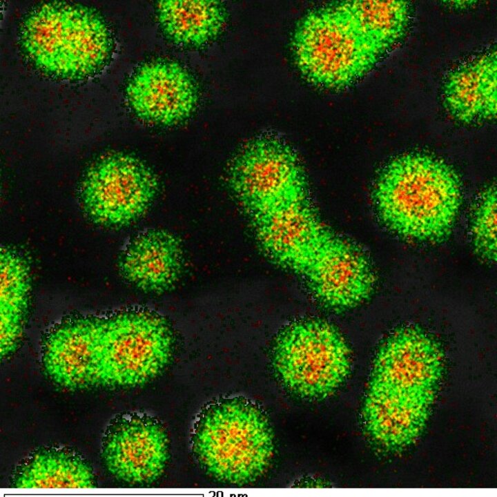
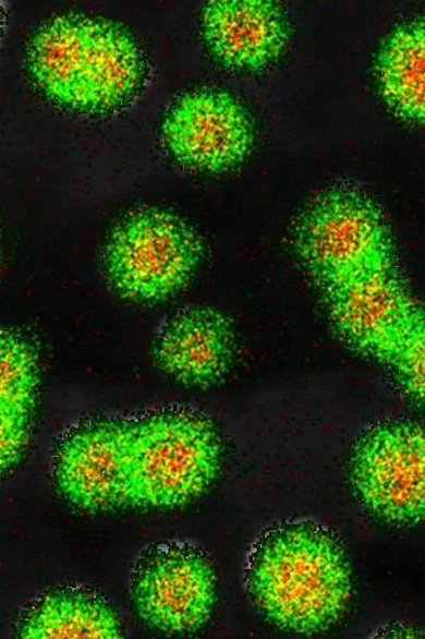
NanoparticlesNanoparticles (0-dimensional nanomaterials) have attracted immense interest because of their physical, chemical and optical properties that can be useful for many applications. Within the PMP group, there are several activities focussing on novel synthesis routes of nanoparticles. For example, new plasma-based processes are being developed for high throughput synthesis of silicon nanoparticles. Moreover, strategies are being developed to prepare supported nanoparticles of noble metals through atomic layer deposition (ALD). One example is the preparation of bimetallic core/shell nanoparticles entirely by ALD. These metallic nanoparticles have applications in the field of catalysis but they can also be used as catalyst particles for CNT synthesis.Nanowires and carbon nanotubesCarbon nanotubes (CNTs) are graphene sheets rolled up into cylinders with diameters as small as one nanometer and are considered to be 1-dimensional nanomaterials. There are two families of CNTs: single-walled CNTs (SWNTs) and multi-walled CNTs (MWNTs). A SWNT can be either metallic or semiconducting depending on its structural parameters. Within PMP, we implement catalytic CVD processes for CNT synthesis by exposing catalyst nanoparticles like Fe, Co, Pt to a carbon feedstock gas such as C2H5OH at high temperature (typically 600-1200°C). The desired CNTs are grown from the catalyst particles and their diameter depends on the size of the catalyst particles.
Within PMP, research is also carried out with respect to the functionalization and passivation of nanowires. These nanowires are being prepared within the Photonics and Semiconductor Nanophysics (PSN) group. For example, we try to passivate semiconducting nanowires to reduce surface recombination or we functionalize nanowires with nanoparticles.
Graphene and other 2D materials
Graphene is a monolayer of carbon atoms arranged in a hexagonal lattice. It is considered to be a 2-dimensional material, since it has no out-of-plane bonds. Graphene can be synthesized on a large scale using a process called chemical vapor deposition (CVD). For CVD growth of graphene, a copper substrate is heated in a tube furnace to around 1000°C and then exposed to a mixture of hydrogen and methane. Carbon atoms from methane adsorb on the copper surface and bond to other carbon atoms in a hexagonal pattern forming a monolayer of graphene. Within PMP, we investigate how different growth parameters influence the growth and quality of graphene.
Besides graphene, other 2D materials such as transition-metal dichalcogenides (TMDs) will be studied, most notably molybdenum disulphide (MoS2).
One of the research areas with the Plasma & Materials Processing (PMP) group is to study the growth and synthesis of 0D, 1D and 2D nanomaterials such as nanoparticles, nanowires and nanotubes, and graphene and other 2D matierals for various applications ranging from catalysis to electronic devices.
NanoparticlesNanoparticles (0-dimensional nanomaterials) have attracted immense interest because of their physical, chemical and optical properties that can be useful for many applications. Within the PMP group, there are several activities focussing on novel synthesis routes of nanoparticles. For example, new plasma-based processes are being developed for high throughput synthesis of silicon nanoparticles. Moreover, strategies are being developed to prepare supported nanoparticles of noble metals through atomic layer deposition (ALD). One example is the preparation of bimetallic core/shell nanoparticles entirely by ALD. These metallic nanoparticles have applications in the field of catalysis but they can also be used as catalyst particles for CNT synthesis.Nanowires and carbon nanotubesCarbon nanotubes (CNTs) are graphene sheets rolled up into cylinders with diameters as small as one nanometer and are considered to be 1-dimensional nanomaterials. There are two families of CNTs: single-walled CNTs (SWNTs) and multi-walled CNTs (MWNTs). A SWNT can be either metallic or semiconducting depending on its structural parameters. Within PMP, we implement catalytic CVD processes for CNT synthesis by exposing catalyst nanoparticles like Fe, Co, Pt to a carbon feedstock gas such as C2H5OH at high temperature (typically 600-1200°C). The desired CNTs are grown from the catalyst particles and their diameter depends on the size of the catalyst particles.
Within PMP, research is also carried out with respect to the functionalization and passivation of nanowires. These nanowires are being prepared within the Photonics and Semiconductor Nanophysics (PSN) group. For example, we try to passivate semiconducting nanowires to reduce surface recombination or we functionalize nanowires with nanoparticles.
Graphene and other 2D materials
Graphene is a monolayer of carbon atoms arranged in a hexagonal lattice. It is considered to be a 2-dimensional material, since it has no out-of-plane bonds. Graphene can be synthesized on a large scale using a process called chemical vapor deposition (CVD). For CVD growth of graphene, a copper substrate is heated in a tube furnace to around 1000°C and then exposed to a mixture of hydrogen and methane. Carbon atoms from methane adsorb on the copper surface and bond to other carbon atoms in a hexagonal pattern forming a monolayer of graphene. Within PMP, we investigate how different growth parameters influence the growth and quality of graphene.
Besides graphene, other 2D materials such as transition-metal dichalcogenides (TMDs) will be studied, most notably molybdenum disulphide (MoS2).