TCOs and thin film encapsulation
TCOs
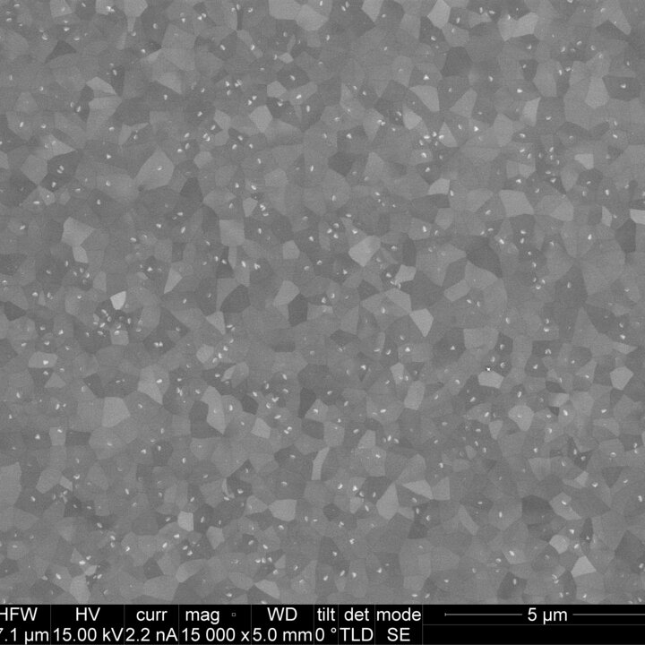
The Plasma & Materials Processing (PMP) group has significant expertise in the deposition of thin films of transparent conducting oxides (TCOs). TCOs are widely used as electrodes for opto-electronic devices, such as solar cells and LEDs, since they exhibit the unique combination of high transparency (> 80%) in the visible range and low electrical resistivity (~ 10-4Ω∙cm-1). These properties are achievable since TCOs have wide band-gaps (> 3 eV) and a significant free carrier density and a high mobility. Extrinsic doping is commonly applied to improve the electrical properties. At PMP, specific attention is given to the deposition of Al- and B-doped ZnO and Sn-doped In2O3 (ITO), both by the expanding thermal plasma chemical vapour deposition (ETP-CVD) and the atomic layer deposition (ALD) method. ETP-CVD provides layers with a resistivity as low as 3×10⁻⁴Ω∙cm-1 for 100 nm film thickness. Furthermore, it is employed at industrial level for its high growth rates, and the plasma causes negligible ion bombardment at the substrate, thereby preserving the quality of the underlying device. ALD provides high uniformities for large areas, high conformality on 3D structures, as well as accurate control of doping levels and film thicknesses. We aim to develop a high level of understanding of the thin-film growth mechanisms, for example to modify the spatial distribution of dopants in thin films during these processes, since the microstructure and chemical composition of the films defines their optical and electrical properties. This includes probing the gas phase- and surface-reactions, and surface diffusion mechanisms that are involved in film growth. The opto-electronic properties of TCOs are inextricably linked – for instance, a high dopant concentration can cause transmission losses in the infra-red region – and so it is paramount to understand how the material parameters can be tailored for the desired application.
Thin film encapsulation
Another branch of research carried out at PMP addresses the investigation of thin-film encapsulants or barrier layers for large area (flexible) electronics, such as thin film solar cells and organic LEDs. For example, in the case of organic LEDs, one of the challenges in device engineering is to massively reduce the sensitivity of both the organic semiconductor and low work function cathode towards H2O vapor and O2 by applying thin-film encapsulants. These latter often consist of stacks of alternating organic and inorganic layers.
At PMP, several deposition techniques are explored to deposit both inorganic and organic layers, such as (Plasma Enhanced) Atomic Layer Deposition (PE-ALD), plasma enhanced chemical vapor deposition (PE-CVD), initiated chemical vapor deposition (i-CVD) and molecular layer deposition (MLD). Water permeation is found to occur through local pinholes/defects present on the surface of the encapsulated device as well as through the (bulk) nano-porosity of the barrier. For this reason, we also study the barrier layers by means of ellipsometric porosimetry (EP). EP is a technique based on adsorption/desorption studies performed using different probe molecules with a specific kinetic diameter, which allows to detect and quantify the residual nano-porosity in the layer.
Next to ellipsometric porosimetry, Electrochemical Impedance Spectroscopy (EIS) allows probing the pore size distribution by following the permeation of both water and ions with selected hydrated ion shell size.
TCOs
The Plasma & Materials Processing (PMP) group has significant expertise in the deposition of thin films of transparent conducting oxides (TCOs). TCOs are widely used as electrodes for opto-electronic devices, such as solar cells and LEDs, since they exhibit the unique combination of high transparency (> 80%) in the visible range and low electrical resistivity (~ 10-4Ω∙cm-1). These properties are achievable since TCOs have wide band-gaps (> 3 eV) and a significant free carrier density and a high mobility. Extrinsic doping is commonly applied to improve the electrical properties. At PMP, specific attention is given to the deposition of Al- and B-doped ZnO and Sn-doped In2O3 (ITO), both by the expanding thermal plasma chemical vapour deposition (ETP-CVD) and the atomic layer deposition (ALD) method. ETP-CVD provides layers with a resistivity as low as 3×10⁻⁴Ω∙cm-1 for 100 nm film thickness. Furthermore, it is employed at industrial level for its high growth rates, and the plasma causes negligible ion bombardment at the substrate, thereby preserving the quality of the underlying device. ALD provides high uniformities for large areas, high conformality on 3D structures, as well as accurate control of doping levels and film thicknesses. We aim to develop a high level of understanding of the thin-film growth mechanisms, for example to modify the spatial distribution of dopants in thin films during these processes, since the microstructure and chemical composition of the films defines their optical and electrical properties. This includes probing the gas phase- and surface-reactions, and surface diffusion mechanisms that are involved in film growth. The opto-electronic properties of TCOs are inextricably linked – for instance, a high dopant concentration can cause transmission losses in the infra-red region – and so it is paramount to understand how the material parameters can be tailored for the desired application.
Thin film encapsulation
Another branch of research carried out at PMP addresses the investigation of thin-film encapsulants or barrier layers for large area (flexible) electronics, such as thin film solar cells and organic LEDs. For example, in the case of organic LEDs, one of the challenges in device engineering is to massively reduce the sensitivity of both the organic semiconductor and low work function cathode towards H2O vapor and O2 by applying thin-film encapsulants. These latter often consist of stacks of alternating organic and inorganic layers.
At PMP, several deposition techniques are explored to deposit both inorganic and organic layers, such as (Plasma Enhanced) Atomic Layer Deposition (PE-ALD), plasma enhanced chemical vapor deposition (PE-CVD), initiated chemical vapor deposition (i-CVD) and molecular layer deposition (MLD). Water permeation is found to occur through local pinholes/defects present on the surface of the encapsulated device as well as through the (bulk) nano-porosity of the barrier. For this reason, we also study the barrier layers by means of ellipsometric porosimetry (EP). EP is a technique based on adsorption/desorption studies performed using different probe molecules with a specific kinetic diameter, which allows to detect and quantify the residual nano-porosity in the layer.
Next to ellipsometric porosimetry, Electrochemical Impedance Spectroscopy (EIS) allows probing the pore size distribution by following the permeation of both water and ions with selected hydrated ion shell size.