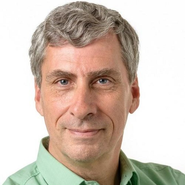
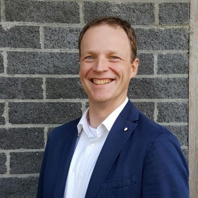
Rob Willekers and Rogier Verberk, NOMI collaboration
IF YOU WANT TO PUSH A NEW TECHNOLOGY, YOU NEED A CONSTANT INFLOW OF KNOW-HOW
At TNO, we focus on projects for customers and go a bit deeper into the technology. At some point, we say, ‘well, that’s fundamental science.’ That’s not for us.”
In the previous High Tech Systems Center newsletter, TU/e’s Henk Nijmeijer and Hamed Sadeghian discussed the development of NOMI (Nano Opto-Mechatronics Instruments), a collaboration which has had major impacts in various fields and the wider Brainport area. In this edition, TNO shares their side of the story.

THINKING OF THE LONG TERM
For Rob Willekers and Rogier Verberk, NOMI represents a technological push: the idea that something new can be brought to the table by combining nano opto-mechatronics with TNO’s existing branches. In November 2017, they teamed up with TU/e HTSC to make this a reality, driving the development of instruments that can image, measure and fabricate devices at the level of atoms. As Program Manager, Rob brings almost 20 years of experience at ASML, while Rogier combines expertise from his various roles as physicist, principal project manager, roadmap leader at QuTech, and now Director Semiconductor Industry.
“Nearly all universities in the Netherlands work together with TNO, but often on a project basis,” Rogier begins. “What’s different here is that we have a long-term vision, aiming to understand each other better and have an idea of where we both want to go.” This includes, for example, regular Science Board meetings in which each discipline defines spearheads that collectively shape NOMI’s future. “It’s good that we have complementarity in the approach. If you don’t take chances, it takes too long. In parallel, if you don’t build on the fundamentals – how it works in the tiniest detail – you have just a single shot. If you fail, you fail miserably.”
Rob agrees. “I like to talk applications with people because then they can be creative. You don’t want to continue on a path if another will be more successful. Fundamental science and market demand need to meet somewhere – there should certainly be room for the building up of knowledge.”
"This is where HTSC comes in, providing a crossroads at which academia and industry can meet..."
This is where HTSC comes in, providing a crossroads at which academia and industry can meet as well as bringing in unique experience in opto-mechatronics. In turn, TNO provides an outlet through which the generated knowledge can be transformed into tangible products that benefit businesses and society. The value has already been demonstrated through the start-up Nearfield Instruments, a spin-off which is beginning to commercialize high throughput scanning probe microscopy developed within NOMI.
Multiple ‘winners’
Alongside bio-medical instrumentation and gravitational wave sensing, semiconductor manufacturing process metrology is a roadmap of NOMI – one in which Rob and Rogier see enormous potential. “In the semiconductor industry,” explains Rob, “there’s a continuous shrinking in device architecture while the manufacture and design of semiconductors is becoming more complex. We see a need to support high-volume manufacturing processes with the correct metrology, not only in designing the processes but in controlling them. It’s clear that there won’t be one clear ‘winner’: we’ll have to make use of multiple technologies and measurements.”

Measuring at the atomic scale is not yet possible for miniaturized devices, but NOMI’s investigations are opening all sorts of doors. Multi-model imaging, for example, is yielding so much information that new data mining and machine learning techniques are inevitable. “The solution for metrology will be a multi-modal, deep learning-assisted multi-measurement head platform, including measurement techniques based on acoustics and optics,” Rob continues. “It would be great to apply acoustic sensing to semiconductors, such as using modeling that detects cracks in oil pipes at the nanometer scale. Some of the companies working on semiconductor devices are also preparing for the quantum era, and there will be a need for metrology there.”
And the biggest challenges that lie ahead? “I’d turn that question around,” says Rogier. “It’s already amazing that we in metrology can keep up with the advancements in lithography, which has been more difficult than ever in the last decade. If you zoom out, the sheer fact that scanning probe is considered a metrology technique is a big step for this ecosystem.” Thanks to the combined efforts of TNO and HTSC, this technology has been sped up and can be used as a primary technique for the first time.
Thinking further on the challenges, Rob mentions the ever increasing need for more accurate overlay performance and measurement. “The large industry challenge is to be able to align product layer to product layer, which is where we also see potential for multimodal imaging , including acoustic techniques. I would boldly say that if we can show a proof-of-concept for that within two years, I’d be very happy. It may take longer but it’s good to have it as a goal!” Rogier laughs. “Make it happen!”
Keeping the Netherlands on the map
In the long term, says Rob, “my dream is the multi-model platform, a combination of the right technologies that can give the right answers within a holistic metrology approach – accuracy combined with speed.” “I share the same dream!” adds Rogier. “And it would be great for the ecosystem to have a second market outlet, maybe in the bio-medical domain. The semiconductor applications are so advanced that any second market would be good.”
"Students are critical as it’s all about having the next generation of talented people,” agrees Rogier
Indeed, the future looks bright for NOMI: market traction has been achieved and investors are willing to support a start-up company working in a mature and challenging industry. The reputation of the Netherlands for equipment manufacturing plays an important role. Rob: “Talent makes the difference and having an application in mind allows creative people to think outside the box. As Eindhoven is well-positioned within the Brainport region, there’s the unique opportunity to take a close look at real applications and be both innovative and realistic.”
By connecting the university to all areas of industry, such as by providing PhD positions within companies, HTSC has a vital role to play here. “Students are critical as it’s all about having the next generation of talented people,” agrees Rogier. “We deliver a unique environment, which is the reason that students from abroad want to come to the Netherlands and be inspired by our leading industry. This must be a sustainable system and we should never forget that it needs continuous investments and attention. Once you lose it, you can never get it back.”
For more information about their work, please contact Rob or Rogier .
For more information about the NOMI collaboration: an interview with the professors Henk Nijmeijer and Hamed Sadeghian.