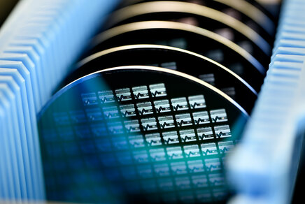
Enabling future nanoelectronics with plasma-assisted atomic layer deposition
‘Plasma-assisted atomic layer deposition’, or plasma ALD in short, is becoming vital for making the thin films that are needed in present-day and future nanoelectronics. As the name suggests, in this method you basically stack layers of atoms on top of each other, to build up the film with extreme precision.
In addition, you use a so-called plasma during the process. A plasma can be seen as a gas that is ionized by an electromagnetic field, just like the gas in a neon lamp. Plasmas have unique properties that are key for making the thin film. A downside, however, is that plasmas are quite complex. They consist of many different particles and their impact on the process is largely unknown. Or at least, their impact was largely unknown, before Arts started his research project.
In his work, he provided key insights into the role of the different plasma species during plasma ALD. For example, using an entirely new and powerful method, he showed that the reactive particles called radicals can move much further into deep 3D structures than previously assumed.
In addition, he revealed how the charged particles that hit the surface can influence the process and how this influence can be controlled. This is all valuable information for new applications of plasma ALD. In conclusion, his research has further advanced plasma ALD as a processing technique, which is especially important for making faster, cheaper, and more sustainable computer chips.
Karsten Arts received his doctorate September 15th on his thesis titled: ‘Conformality and the role of ions during plasma-assisted atomic layer deposition’. Supervisors: prof.dr.ir. Erwin Kessels, Dr.ir. Harm Knoops
Latest news