Doping control at the atomic scale in III-V semiconductors
Douwe Tjeertes defended his PhD thesis at the department of Applied Physics and Science Education on March 17th.
![[Translate to English:]](https://assets.w3.tue.nl/w/fileadmin/_processed_/4/c/csm_Tjeertes%20Banner%20image_796a505108.jpg "[Translate to English:]")
Semiconductor devices can be found in smartphones, LEDs, solar panels, and a range of other technologies that we use every day. To make materials that are suitable for semiconductor devices, extra atoms, known as doping or impurity atoms, can be added to the materials, changing their properties in the process. As devices get smaller and smaller, we are approaching a point where just a few atoms, or even a single atom, can change the properties of a material in a drastic way. For his Phd research, Douwe Tjeertes looked at ways to precisely monitor and control the doping of gallium arsenide with bismuth and nitrogen atoms.
Gallium arsenide (GaAs) is common semiconductor material, which is used for optical and electronic applications. Bismuth and nitrogen impurities have multiple effects when placed in GaAs as doping atoms, which can be beneficial for applications such as lasers. For such applications, it is important that the impurity atoms are homogenously spread throughout the material, but this is not always the case.
Marking atoms by hand
For his PhD research, Douwe Tjeertes and his collaborators studied doped semiconductor materials to see how they are dispersed in the material.
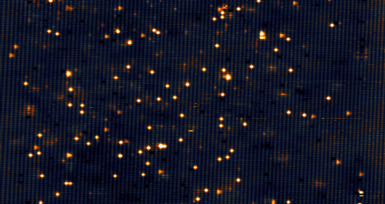
To visualize the atoms in doped semiconductor materials, Tjeertes used turned to scanning tunnelling microscopy (STM). In this approach, an atomically sharp metal tip scans over the surface of a semiconductor material containing doping atoms. A quantum mechanical current can be then be measured and used to construct an image of the sample of interest, and hence allows for the observation of the doping atoms.
In numerous images, Tjeertes marked the position of over 20,000 atoms by hand, after which analysis of the images revealed that the atoms were not placed randomly in the material. Instead, he noticed that the bismuth atoms sit close to each other and avoid the nitrogen atoms. The exact placement of the bismuth atoms seems to be strongly dependent on the way the material is grown.
Complexes
Until a recent discovery, it was impossible to change the properties of a semiconductor after it has been grown, For GaAs grown with nitrogen (N) impurities, the effects of the nitrogen impurities can be nullified by exposing the grown material to a plasma of atomic hydrogen (H).The hydrogen binds to the nitrogen atoms and creates complexes of N and H. It is possible to remove these complexes again by heating the material or applying energy at a local scale. So, in this way it is possible to tune the properties of the material again and again.
Tjeertes looked at these N-H complexes with atomic resolution and was able to observe different types of complexes in the grown semiconductor. He was also able to manipulate the complexes with the STM tip, making it possible to switch one of them between two different states. For another complex, he removed it completely, indicating it’s possible to remove the hydrogen from N-H complexes. This shows the ultimate control over these complexes since we can remove at the atomic level.
Tjeertes research show that STM is an excellent tool for the observation and even manipulation of semiconductor dopants at the atomic scale. His work provides a deeper understanding of doping atoms, which can be used for the fabrication of future devices.
Title: Doping control at the atomic scale in III-V semiconductors. Supervisor: prof. dr. P.M. Koenraad.
Media contact
Latest news