New integrated device for nanometer-scale sensing
‘Nano-metrology lab on a chip’ within reach thanks to new compact, optical sensor.

Researchers at Eindhoven University of Technology have developed a new, integrated optical sensor that provides increased resolution in measurements and paves the way for fully integrated and compact optical sensors including lasers and detectors for on-chip sensing platforms. Such sensors could play a pivotal role in accurate displacement and force measurements at the nanoscale, which is crucial for microchip and nanodevice design and evaluation. This research has been published in Nature Communications.
In the age of nanoelectronics, precision is the order of the day. For example, nanostructures can be monitored with nano-optical instrumentation – tiny, light-based systems that measure the smallest of surface variations, forces and movements. As resolution and speed are essential, optical read-out sensors based on optomechanical systems are frequently used in sensing applications such as in atomic force microscopes (AFMs). These devices generate sub-nanometer resolution images by measuring the laser light reflected by the deflection of a cantilever over a surface of interest.
However, traditional laser-based approaches such as those in AFMs can be bulky, which along with the demand for lower cost and higher resolution, motivates the need for an alternative approach. Thanks to developments in nano-optomechanical systems (NOMS), compact optical sensors for the measurement of motion, force, and mass at the nanoscale are achievable. A limiting factor though is the need for a tuneable laser with a narrow linewidth, which can be difficult to adequately incorporate on a device.
To circumvent this issue, Tianran Liu, Andrea Fiore, and colleagues from the Institute for Photonic Integration at TU/e designed a new optomechanical device with a resolution of 45 femtometers (which is about 1/1000 the size of the smallest atom) in a measurement time of a fraction of a second. Crucially, the device has an ultrawide optical bandwidth of 80 nm, removing the requirement for a tuneable laser.

Waveguides and large wavelength range
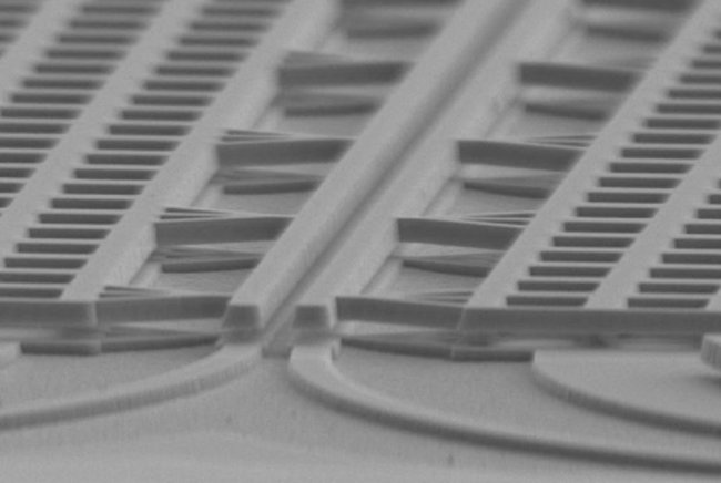
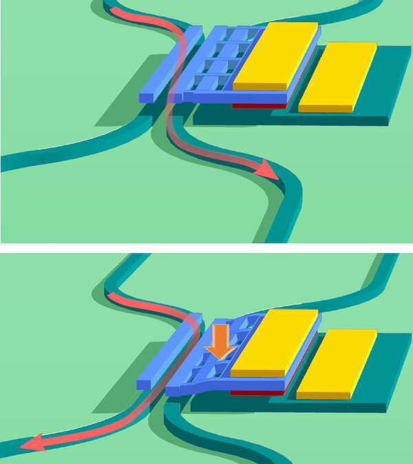
The sensor is based on an indium phosphide (InP) membrane-on-silicon (IMOS) platform, which is ideal for including passive components such as lasers or detectors. The sensor itself consists of four waveguides – structures that restrict light signals to a particular path and direction – with two waveguides suspended above two output waveguides. When a suspended waveguide is pushed towards the output waveguides on the InP membrane, the relative amount of signal carried by the output waveguides varies. Fabrication takes place via a series of lithography steps to define the waveguides and cantilever, and the final sensor consists of the transducers, actuator, and photodiodes.
One of the key advantages of this sensor is that it operates in a large range of wavelengths, which eliminates the need for an expensive laser on the device. In terms of cantilever deflection, the sensor also replicates the resolution of cantilevers in traditional, but bulky AFMs. Using this new device as a foundation, the researchers plan on developing an entire “nanometrology lab” integrated on a chip that can be used for semiconductor metrology and help in the design of the next generation of microchips and nanoelectronics.
Full paper: Tianran Liu et al., “Integrated nano-optomechanical displacement sensor with ultrawide optical bandwidth”, Nature Communications, (2020), doi: 10.1038/s41467-020-16269-7.