Producing materials to help break the electronics scaling limit
One step closer to smaller, more cost-effective electronic devices made of 2D materials.
PhD candidate Saravana Balaji Basuvalingam at the TU/e Department of Applied Physics developed a new approach to grow a library of so-called TMC materials with various properties at low-temperature in a controlled and effective way, bringing the world one step closer to move beyond silicon-based semiconductor devices.
As the amount of data produced by humanity growth exponentially, with it comes the demand for smaller, faster and cheaper electronic devices to process these data. To address this demand, the semiconductor industry is continuously searching for ways to scale devices below 3 nm. This scale is an important barrier for the industry, because it is near the limits of what can be done with silicon (Si), the most commonly used material for electric circuits. Below that scale, silicon-based devices often suffer from poor performance.
Certain 2D materials, of which graphene may be the most well-known example, offer the promise to solve this scaling issue. Characteristic of these materials is that each layer of atoms is free-standing on the layer of atoms below, without any bonds connecting the layers. The 2D materials classified as transition metal chalcogenides (TMCs) has gained attention for their excellent electrical properties and thickness of less than 1 nm, enabling device performances similar to Si-based devices and a great potential for scaling.
Turning promise into potential
However, several synthesis limitations restrict the implementation of TMCs in industry in a cost-effective way. Basuvalingam’s research aimed to solve most of these technical limitations, such as growing the TMCs in a large enough area, at low temperature and with good material property control. To do so, he used a thin-film approach known as the atomic layer deposition (ALD) method. ALD is one is the prominent methods to facilitate the reduction of device dimensions in the semiconductor industry, and the method had already been studied for TMCs which exhibit semiconducting properties.
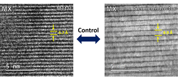
Basuvalingam was the first to study ALD to grow 2D TMCs with both semiconducting and metallic properties in a large area at low temperatures, and the first to achieve control over TMCs’ material composition using thin-film synthesis. His approach also made it possible to grow TMCs in a 200mm wafer and to achieve control of the material properties between metallic and semiconducting.
His work expands the library of materials that can be grown using a thin-film method and helps us get one step closer to smaller, more cost-effective electronic devices made of 2D materials.
Title of PhD-thesis: Atomic Layer Deposition of Low-Dimensional Transition Metal Di- and Tri-Chalcogenides and their Heterostructures. Funded by: European Research Council (ERC). 1st promoter: Ageeth A. Bol. 2nd promoter: Wilhelmus (Erwin) M. M. Kessels.