Enhancing IC fabrication monitoring with soft X-ray computational techniques
Stefan Eijsvogel defended his PhD thesis at the Department of Electrical Engineering on March 26th.
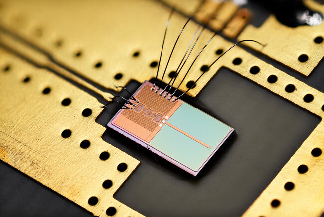
Nowadays, society heavily relies on electronic devices for work, transportation, communication, entertainment, and more. To continually enhance these devices, whether through reduced power consumption or increased memory capacity, the core components - integrated circuits (ICs) - must be manufactured with increasingly smaller structures and finer details. Monitoring the fabrication process of ICs with precision is crucial to detect production defects and calibrate the process for subsequent batches, thus ensuring the production of functional ICs. Failure to do so risks the production of faulty ICs. In his PhD research Stefan Eijsvogel has developed computational techniques capable of accurately estimating the shape and material properties of these structures, representing the particular details of an IC, during the fabrication process.
The advancements in the performance of electronic devices such as reduced power consumption are of great interest for a sustainable society. Nevertheless, these advancements only become truly effective when a widespread adoption of these electronic devices is possible for society. This widespread adoption depends on the rapid production of next-generation ICs within the fabrication error tolerances. Here, the fast and accurate monitoring of the structures that form an ICs is vital, since it provides the necessary information to perform a calibration of the fabrication process such that fabrication errors can be reduced or even prevented.
Monitoring of ICs
Currently, an effective monitoring approach is based on illuminating the structures that form an IC by focused visible light and then measuring and analyzing the electromagnetic response. The mathematical analysis of the measured response is vital for recovering essential details of the shape and material properties of these structures. This process can be compared to taking photos and then thoroughly analyzing the contents of the photos.
The fine details of next-generation ICs are in the range of only a few nanometers, which cannot be observed by visible light. This problem can potentially be resolved by replacing the visible-light illumination by soft X-rays with a forty-fold smaller wavelength. However, the electromagnetic responses of the structures of ICs are barely measurable, due to the near-transparent behavior of the structures’ materials under soft X-ray illumination. This leads to response measurements with a poor quality. Further, it is not possible to focus the soft X-rays, since soft X-rays are almost completely absorbed by lenses or mirrors. As a consequence, the existing approach for monitoring by visible-light illumination cannot be directly applied to the soft X-ray case. This makes the fabrication monitoring of next-generation ICs by soft X-rays challenging.
Towards soft X-ray monitoring
In the Electromagnetics group of the Electrical Engineering department, Eijsvogel has extended and developed various methods that together form a computational technique for accurately and robustly estimating the shape and material properties of the structures, which together represent parts of an IC, by soft X-ray illumination. These methods cover accurate and computationally efficient ways to analyze and detect the scattering for a large class of shapes acting as the structures of an IC.
The research took place at the Electromagnetics Group at the Department of Electrical Engineering. Further, this research is part of the perspective program of NWO-TTW with the name LINX (Lensless Imaging of 3D Nanostructures with soft X-rays).
Thesis title: Forward and inverse scattering by parametrized finite scattering objects in the soft X-ray regime. Promotor: Martijn van Beurden. Co-promotor: Roeland Dilz.