"Exact placement of atoms can drive future chip innovations"
Area-selective atomic layer deposition is set to be a leading technique when it comes to making the advanced computer chips of the future, according to TU/e researcher Adrie Mackus.
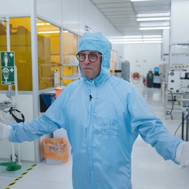
Computer chips. Microchips. Silicon chips. The tiny computing devices that drive your smartphone, laptop, and TV go by many names, and there are a lot of methods to make these chips. One such method is atomic layer deposition (ALD) – the process by which atoms are neatly placed on a surface to build chips. For the past 20 years it has proved its worth in the microchip manufacturing toolbox, but now it needs renewal. With the nanoelectronics age approaching fast, and the need to be more sustainable, more accurate iterations of ALD are needed to build smaller and smaller chip structures. Adrie Mackus and his colleagues at TU/e are leading the way in ALD developments, with their focus being on one that is area-selective. Why could solving the puzzle of ‘AS-ALD’ revolutionize how the industry makes our future chips?
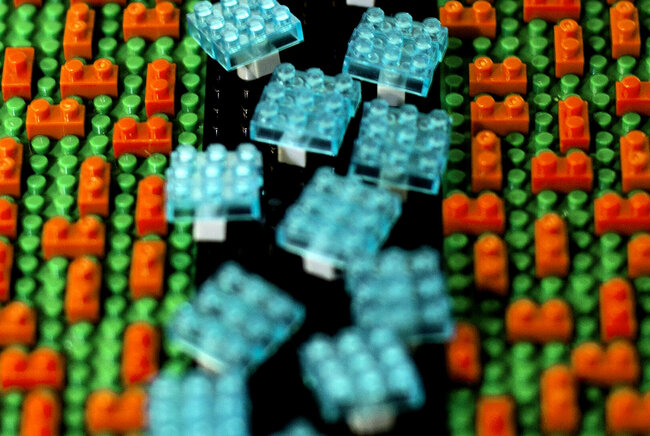
Brick by brick. Layer by layer. From bottom to top. All these phrases surmise to an extent the process of building a house or a microchip.
“There is a subtle difference though between building a home with bricks and a computer chip with molecules,” says Adrie Mackus, associate professor at the Department of Applied Physics and Science Education and part of the recently launched TU/e Future Chips Flagship initiative.
Mackus is working on a technique known as atomic layer deposition (ALD), which has been a cornerstone technique to make microchips over the last two decades.
What is atomic layer deposition (ALD)?
While the name ‘atomic layer deposition’ suggests that individual atoms are arranged one-by-one to make chips, the technique is a little more involved.
To be precise, ALD is a thin-film deposition technique whereby a very thin layer of material is deposited on top of another layer below it. Central to the technique is the use of chemical reactants in a gas phase.
ALD consists of two key steps – the precursor step and the co-reactant step. During the precursor step, a molecule (perhaps a metal organic molecule) containing an atom that needs to be deposited is placed on the surface. This molecule can more easily bind to the surface than the individual atom.
Then, during the reactant step, the deposited precursor molecule is exposed to a reactant, such as water or oxygen. This removes the unwanted segments of the molecule, leaving the desired atom deposited as a layer.
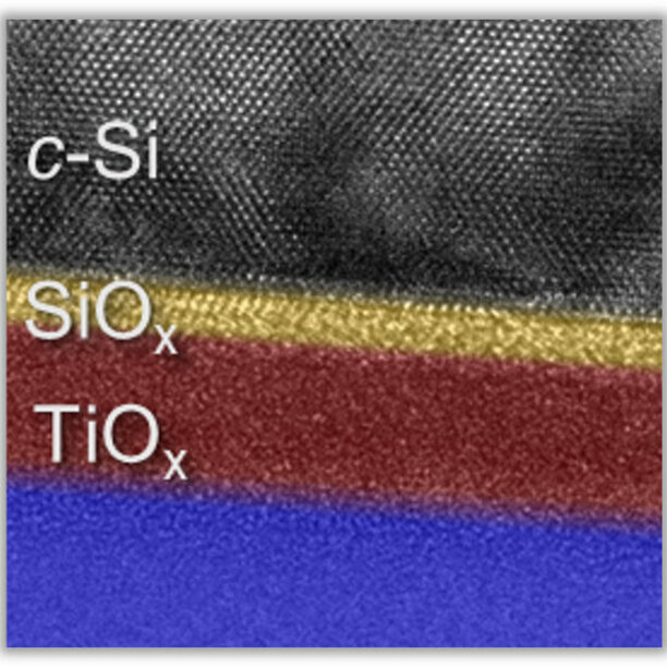
Image: Bart Macco - adapted from "Explorative studies of novel silicon surface passivation materials : Considerations and lessons learned", Sol. Energy Mater. Sol. Cells. 188 (2018) 182–189. DOI: 10.1016/j.solmat.2018.07.003.
The how and how old
Making tiny computer chips with ALD in industry is rather involved. So, when asked to explain how ALD works, Mackus turns to the ‘house building’ analogy.
“When you’re building a house, first you put down the bricks and then the mortar. Ignoring windows or doors, in essence, there are two building materials in each brick layer. It’s the same in ALD where we alternate two chemicals to make an atomic layer.” [See highlight block above for more technical details.]
In 2024, ALD celebrates a major milestone. “This summer it’s ALD’s 50th birthday,” says Mackus. “It took some time for the technique to be added to the microchip manufacturing toolbox, but now it’s one of the go-to tools.”
The need for ALD change
ALD can put down a certain number of atomic layers, which is a major advantage, but it’s not as simple as just placing flat layers on top of flat layers. Computer chips are made almost completely top-down, which involves first deposition, followed by patterning and etching. That’s as if you build a house by putting down a cube of bricks and then remove all the bricks that you don’t need, instead of locally making walls and floors.
“When you zoom in on a computer chip, you’ll see different “rooms. Sometimes you want to deposit materials at the floor of the living room but not in the kitchen,” notes Mackus.
“A computer chip consists of a stack of hundreds of thin films (each could between 10 and 100 atomic layers), but the repeated deposition and etching wastes a lot of material too,” says Mackus. “Added to that, future computer chips will rely on building tiny nanoscale structures. Basically, all of this means that we need more precise placement of smaller building blocks.”
How exactly does area-selective ALD work?
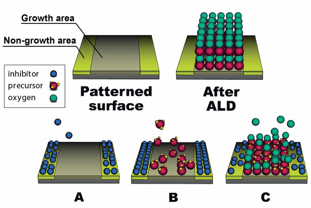
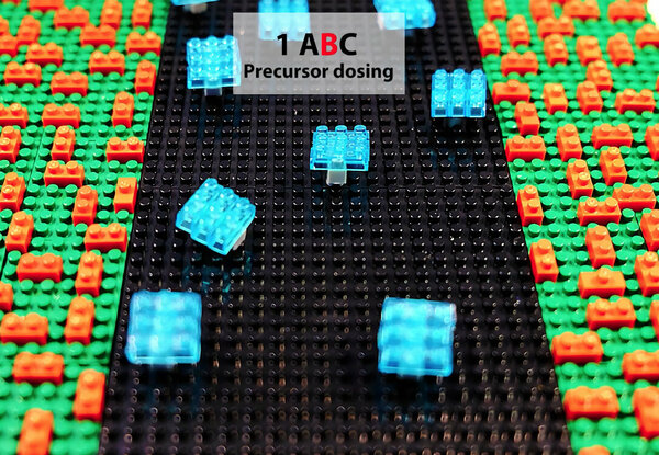
The starting point in AS-ALD is a surface with two different materials, and the aim is to deposit materials on one surface (the growth area) and not on the other areas (the non-growth areas).
In comparison to traditional ALD, Mackus’ approach to AS-ALD includes an additional step during which inhibitor molecules are absorbed on the non-growth areas (Step A). The aim of the inhibitor molecules is to prevent absorption of the precursor molecules on the non-growth areas.
Once the inhibitor molecules are in place, AS-ALD follows the precursor step (B) and then the co-reactant step just as for ALD. During the co-reactant step (C), the inhibitor molecules on the non-growth areas are also removed.
Image: Adrie Mackus
Time to be area-selective!
ALD has played a leading role in chip fabrication, but change is afoot, driven by advancements in technology and the need to be more sustainable.
As microchips embrace the nanoscale, ALD needs to move with the times to build nanoscale structures. Enter area-selective atomic layer deposition, or AS-ALD.
“AS-ALD has been around for about 20 years, and work in the field even stagnated a decade ago,” says Mackus. “It’s become popular again, and I believe the precise placement of atoms (also known as a bottom-up approach) can drive future chip innovations.”
With area-selective in the name, AS-ALD focuses on depositing atoms on specific areas only. In comparison to ALD, it’s well-suited to depositing or aligning structures at the nanoscale. To facilitate area-selective deposition, Mackus and his colleagues have led the way in innovating the technique.
“To make future chips with state-of-the-art transistors, we need to build features only a few nanometers in size, as well as complex three-dimensional structures. If you need to deposit in every crack and hole in a three-dimensional structure, you cannot use large molecules of two to three nanometers in size. We need tiny molecules to help build tiny structures, and our starting point is that of small molecule inhibitors that block off certain areas of the chip from deposition.”
Moving to the small molecule-approach of AS-ALD also lowers the threshold for industry to change to this technology as it’s possible to work with small molecules in gas-phase in vacuum systems and avoid working in solution. “AS-ALD could be huge for industry, but it’s about making the technique robust and reliable, as well as easy to implement,” adds Mackus.
Chasing the solution to the puzzle
In terms of the future, Mackus has one main goal. “We want to solve the puzzle of AS-ALD, but to solve the puzzle, we need to find the puzzle pieces.”
The puzzle pieces that Mackus is referring to here relate to how to make sure that all the inhibitor molecules behave in the same way, that the inhibitors molecules block every precursor molecule coming in, and to find inhibitor molecules that work for every material that we want to deposit.
Added to that, in his ERC starting grant-funded project, Mackus is exploring ways to deposit atoms on a surface with any orientation. “To date, the focus has been on depositing on flat surfaces, but future chips will need complex three-dimensional structures. Stacking devices on top of each other is more commonplace in memory chips, but also logic chips are going in that direction, which means that techniques that can achieve this are needed.”
And Mackus is confident that he and his colleagues’ findings will lead to great things. “We hope to change chip manufacturing by helping industry build the nanoscale landscapes of our future chips.”
Further information
To achieve his ALD plans, Mackus is working within the Plasma & Materials processing group at the Department of Applied Physics and Science Education, of which Professor Erwin Kessels is the group leader. Currently, his team is made up of three postdoctoral researchers, seven PhD researchers, and several master’s students.
Check out the website Atomic Limits for updates on the latest advancements from Mackus and his colleagues on ALD.
You can also read a series of blog entries there in relation to AS-ALD. One entry covers fully self-aligned vias, which is proposed as the ‘killer application’ for AS-ALD. The second in the series looks at metal-on-metal area-selective deposition, and the final entry explores the AS-ALD of diffusion barriers for interconnect technology.
Why we strengthen our key position on chips
In the coming years, TU/e will expand its key position in Dutch academia in the field of semiconductors with its Future Chips flagship. With the initiative, the university is giving a boost to the development of chip technology to accelerate the creation of solutions to the major societal, economic and geopolitical challenges in this field.
Watch the video and discover why we are the chip university in the Netherlands.
Media contact
Latest news