Below mentioned Graduation projects are available at PhI group.For detailed information on these, and other possibilites, please contact the person(s) mentioned.
High speed photonic ICs
GRADUATION PROJECT: High speed photonic ICs
Track: Connected World
Group: PhI
Mentor: W. Yao
Context:
Photonic integrated circuits have emerged as a promising solution for alleviating the bandwidth bottleneck in modern computing systems and data networks. Indium phosphide (InP) circuits enable the highest performance and have the crucial advantage of allowing the monolithic integration of lasers, amplifiers and modulators. The challenge for Terabit/s transmitter and receiver circuits will be to increase the density of the components.
Assignment M0) High-speed electro-optical modulators are composed of simple functional components such as phase modulators. To enable high-speed operation, the radio-frequency behavior of the phase shifter has to be well understood and its design properly optimized. Appropriate modeling approaches have to be developed that accurately predicts its performance. For this purpose, phase shifter test structures have been designed and fabricated. Within this topic, the student should experimentally characterize the performance of the phase-shifter test structures. In addition, a suitable RF equivalent circuit model needs to be developed, verified through experimental parameter extraction techniques and implemented into ADS or another suitable software solution.
Assignment M3) Arrays of high-speed optical modulators and detectors are integrated in small form-factor semi-conductor chips that exhibit very high integration density. Proximity effects such as electro-magnetic interference between these components start to disturb their performance. We have fabricated samples with closely spaced components and the student’s task is to characterize these samples with respect to electro-magnetic interference.
Activities:
Laboratory experiments, design with photonic CAD tools, analysis and scientific reporting.
Integrated spectrometry
GRADUATION PROJECT: Integrated spectrometry
Track: Care and Cure
Group: PhI
Mentor: Dr. S. Latkowski and Dr.E.A.J.M. Bente
Context:
Precision wavelength control of integrated tunable lasers over a wide range is essential for e.g. gas detection, breath analysis, sensor readout and medical imaging. Precise (up to one part in ten million), fast and repeatable tuning is required using typically 6 to 8 electrical control signals.
Assignment M4) In this assignment you will first investigate theoretical options for algorithms for the laser control and methods for calibrating the laser and its components. One of the options to investigate is the use of special form of neural network called reservoir computing. Then you validate the method experimentally using high speed electronics on an integrated tunable laser for gas detection or medical imaging.
Activities:
Laboratory experiments, neural networks, algorithm development, reporting .

Coupling to photonic integrated circuits
GRADUATION PROJECT: Coupling to photonic integrated circuits
Track: Connected World
Group: PhI
Mentor: Dr. R. Lemos Alvares dos Santos and Dr. X.J.M. Leijtens
Context:
Coupling light into photonic integrated circuits adds considerable cost and complexity in the manufacturing process. We currently explore an innovative combination of flexible waveguides and standard assembly tools to simplify the assembly. The solution is based on an interposer fabricated in TriPleX, where micro optical fibers are fabricated, which enables full passive alignment between the InP PIC and the interposer. Penetration of low cost photonic circuits into new application areas such as in fiber based sensing and structural health monitoring, in datacomms, and metrology becomes conceivable with reduced assembly complexity.
Assignment M5) During this project, you will have the opportunity to get experience with all the fabrication chain of the PICs, from processing to the packaging. You will analyze the coupling efficiencies as a function of the structural parameters of the optical waveguides, taking into account the achievable alignment tolerances, design the next generation of interposers and photonic integrated circuits, and experimentally verify the coupling with dedicated test structures.
Assignment M6) The most demanding assembly task for multi-port PICs is the high-precision (100 nm) alignment of optical waveguides. The PhI group is working on innovative solutions, to use on-chip micro-electro-mechanical systems (MEMS) actuators to achieve this precision alignment. In this project, the student will analyze coupling efficiencies as a function of the structural parameters of the optical waveguides, implement control of the MEMS actuators and experimentally verify with photonic integrated circuits.
Activities:
Laboratory experiments, analysis of optical coupling, photonic IC design, reporting.

Compact laser model
GRADUATION PROJECT: Compact laser model
Track: Connected World
Group: PhI
Mentor: Prof. K.A. Williams
Context:
Laser diodes are essential components in many photonic integrated circuits for communications and new optical sensors. However they are relatively complex and simulation techniques have high computational requirements. To enable the creation of more complex photonic circuits, it is valuable to create fast empirical compact models to identify acceptable operating ranges.During this project, you will have the opportunity to simulation and experimentally measure the most important characteristics of laser diodes, enabling their use in a broader range of photonic ICs.
Assignment M7) Stability regimes for single frequency grating based lasers. Create an algorithm to predict mode hops from one frequency to the next for a grating based laser oscillator. Experimentally verify the model. A successful study would use the model to predict and verify more stable single frequency laser designs.
Assignment M8) Laser threshold minimization for generic integrated Fabry Perot lasers. Create a compact model for laser threshold and power modelling, prepare mask designs for a tape-out and compact model to define test structures for maximum achievable gain, maximum tolerable threshold current densities. This creates an insight into the ultimate limits for laser efficiency with the available components. A successful study will also provide insight in to the relative impact of the various recombination mechanisms.
Activities:
Conceptual model, MPW tape-out, experimental analysis, reporting.

Metal nano-grating couplers
GRADUATION PROJECT: Metal nano-grating couplers
Track: Connected World
Group: PhI
Mentor: Dr. J.J.G.M. v.d. Tol and Dr. Y. Jiao
Context:
Grating couplers are important components for membrane-based integrated photonics. They allow the in- and out-coupling of light from micro-optics to nano-photonic waveguides. These are valuable for on-wafer characterization, fiber-chip-coupling and optical interconnect systems. We have recently proposed a novel metal grating coupler, that uses a silver layer to optically decouple the semiconductor waveguide layer from the substrate underneath, obtaining key advantages and providing design flexibility and enabling fabrication of InP-membrane based circuits that rely on polymer bonding. Additionally, such optical decoupling reduces the optical parasitics into the substrate. The following figures show simulations of the device coupled to an optical fiber and the top view of a linear and non-apodized metal grating coupler.
Assignment M9) Analyze advanced designs of metal grating couplers via simulations. Aspects of fabrication, characterization and experimental analysis are also envisaged. Simulate grating couplers using the Finite-Difference Time-Domain method. The simulations will comprise designs based on subwavelength structures, curved focusing gratings, apodized gratings, and other creative solutions proposed by the student. Design the masks for electron-beam lithography required in the fabrication.
Activities: Design with finite difference time domain EM solvers, prepare a mask for fabrication and characterise in the laboratory. Reporting.

Generation of stabilized frequency combs
GRADUATION PROJECT: Generation of stabilized frequency combs
Track: Connected World
Group: PhI
Mentor: Dr.E.A.J.M. Bente and M. Llorens Revull
Context:
Optical frequency combs are a series of optical frequencies with a well determined frequency interval. When properly stabilized such combs can be used in microwave photonics in e.g. satellite communication systems. Two of such combs together can be combined to do very fast spectroscopic or distance measurements. We are working on miniaturizing and stabilizing laser sources that produce such combs by several orders of magnitude using our integration technology. A frequency comb is characterized by the frequency interval between the comb lines and an offset frequency. The interval stabilization is currently done by applying an RF signals to the laser source. The offset stabilization we would like to implement by linking a comb line to a stable CW laser that can be integrated with the comb source. This has not been demonstrated yet.
Assignment M10) In this assignment you will explore possible stabilization schemes for a frequency comb source. You will then select a design and implement an opto-electronic stabilization system for a frequency comb laser source. You will use this capability to produce a stabilized dual comb system.
Activities:
Laboratory experiments, laser stabilization, electronic systems design, reporting.

Ultrafast optical world
GRADUATION PROJECT: Ultrafest optical pulse amplification and shaping
Track: Connected World
Group: PhI
Mentor: Dr.E.A.J.M. Bente
Context:
Trains of short optical pulses (picoseconds or even shorter) are not only used in tele and data communication but also have many other uses in e.g. in sensing systems, imaging and microwave photonic applications. For this reason we have developed in the PHI group over the years a set of devices to generate and manipulate such pulses an a chip. This allows for the design and fabrication of complex circuits. However an increase in the accuracy of the design capability is required and the response of the integrated optical amplifiers and so called saturable absorber components is essential. Quite a few of the key parameters that are used in the existing theoretical models and which also play an important role in all types of lasers systems, are hard to determine experimentally, so up to now often only theoretical values have been used.
Assignment M11) To determine determine a number of key properties of semiconductor amplifiers and absorbers e.g. electron-hole lifetimes as a function of carrier density and photon density, current injection efficiency, temperature dependence and/or the self-phase modulation parameters. You will combine these results with gain and loss measurements to get to accurate gain, loss and phase modulation descriptions of the amplifiers and absorbers. For these measurements the methods, set-ups and analysis have to be designed and realized. Special test devices may be designed as be part of the work. You will use the latest advanced high resolution spectral analysers and short pulse laser sources. This work is experimentally challenging.
Activities:
Laboratory experiments, semiconductor amplifier modelling, reporting.

Corner mirror
GRADUATION PROJECT: Corner mirror
Track: Connected World
Group: PhI
Mentor: D. Zhao and Dr. X.J.M. Leijtens
Context:
In order to increase the functionality of photonic ICs, it is becoming increasingly important to create more compact designs that better utilize chip area. However, the number of functions that can be realized in a photonic IC is limited by the footprint of building blocks and by the interconnections between them. Normally, low-loss circular waveguide connections are used, but they use a significant chip area because of the rather large bending radius. Total internal reflection (TIR) mirrors can turn sharply, and allow waveguides and devices to be folded, which can increase the device density.
Currently these so-called corner mirrors are not available as design building blocks in the component library. The aim of this project is to design a corner mirror with record performance. Although the principle of operation is rather simple, getting the details right will be a challenging task. A successful building block will be added to the design library and will reduce the overall size of future photonic ICs. Find the optimized design with low mirror loss and good fabrication tolerance. Defeat the current world record, which has a mirror loss around 0.5 dB.
Assignment M12) In this project, you will have the opportunity to get experience with simulation, design, and characterization. Analyze the propagation efficiencies as a function of the structural parameters of the corner mirrors.Design of the next generation corner mirrors and photonic integrated circuits. Experimental verification of the device properties of the designed structures.
Activities:
Literature study, working with simulation software, developing laboratory skills, reporting.

Lighting a nanoworld. Design of an active/passive integrated membrane DBR laser
GRADUATION PROJECT: Design of an active/passive integrated membrane DBR laser
Track: Connected world
Group: PhI
Mentor: V. Pogoretskiy
Context:
Integrated nanophotonics promises to revolutionize sensor and communications technologies, but so far it has been challenging to create light sources in nanophotonic chips. Single wavelength lasers are expected to be a particularly important component in integrated nanophotonics. Promising types of lasers include distributed Bragg reflectors (DBR) such as surface etched gratings and photonic crystal holes (PhC). To decrease the size of the lasers, active/passive epitaxial regrowth on a membrane is used to fabricate these types of lasers which gives us the much smaller footprint and a highly efficient way to couple light from laser to a waveguide. The task of the student will be laser design and optimization.Requirements: Good knowledge of: semiconductor physics, electrodynamics and photonics.
Assignment M13): The student will be performing: Calculations to optimize the optical amplifier and reflector performances.Calculation of laser parameters such as threshold current, electro optical power efficiency and modulation response.Literature review of state of the art. There is an opportunity for students to perform clean room fabrication steps. This should be discussed with the project mentor and supervisor.Measurements of fabricated results. Final report.
Activities:
Design of nanophotonic lasers, predictions of component performance, cleanroom fabrication (optional), measurement and scientific writing.

Grating optimization using genetic algorithms
GRADUATION PROJECT: Grating optimization using genetic algorithms
Track: Connected world
Group: PhI
Mentor: Dr. J.J.G.M. v.d. Tol and Dr. Y. Jiao
Context:
Grating couplers are important components for membrane-based integrated photonics. They allow the coupling of light between micro-optics and nano-photonic waveguides. These are valuable for on-wafer characterization, fiber-chip-coupling and optical interconnect systems. We have recently proposed a novel metal grating coupler, that uses a silver layer to optically decouple the semiconductor waveguide layer from the substrate underneath, obtaining key advantages, providing design flexibility and enabling fabrication of InP-membrane based circuits that rely on polymer bonding. Additionally, such optical decoupling reduces optical parasitic coupling into the substrate.
Assignment M15):Genetic algorithms are powerful tools to achieve unprecedented improvement of performances in photonic devices. This is because they can reach hidden zones, where traditional design logic cannot. The project will study the application of a genetic algorithm in a grating coupler design. Determining the best algorithm, optimizing genetic parameters and obtaining an optimized design will be the main targets. The final goal is to reach nearly 100 % in grating coupling efficiency, as compared to 50% to 75% losses in traditional designs.
Activities:
Develop a genetic algorithm suitable for grating simulation, in combination with commercial photonic simulation tools. Demonstrate an optimized grating coupler design. Reporting.

Plasma etching technique for aluminum based lasers
GRADUATION PROJECT: Plasma etching technique for aluminum based lasers
Track: Connected World
Group: PhI
Mentor: Dr. Y. Jiao and J.P. van Engelen
Context:
Aluminum based materials are popularly used in semiconductor lasers due to its advantage in thermal stability. The lasers made with aluminum materials can have improved stability as temperature changes, and they can also operate at higher temperatures. However this type of material is very difficult to process, because when they are exposed in air or in any oxygen containing environment, they will oxide and no longer be semiconductor anymore. Therefore it is very essential to develop process technologies which can maximally isolate the material to air, and can process the material without oxygen.
Assignment M17) This project will be based on a novel oxygen-free plasma etching technology developed by Dr. Y. Jiao. The original technology was optimized for InP-based materials. The first task of this project is to validate this technology for aluminum based materials, and further optimize it to obtain vertical sidewall and smooth surface. Then the project will be focused on protection techniques for this material. Surface passivation and surface protection techniques are going to be investigated. At the end, the project aims to deliver an optimized etching process as well as the passivation/protection recipes for the aluminum based laser structure. Electron microscopy on the etched ridge geometry, and measurements on the surface recombination rate will be performed to evaluate the outcome of this project.
Activities:
Cleanroom technology development for aluminum based semiconductor materials.

Magnetic claddings for Photonic integrated circuits
GRADUATION PROJECT: Magnetic claddings for Photonic Integrated circuits
Track: Connected World
Groups: PhI (EE) and PNS (TN)
Mentors: Reinoud Lavrijsen (TN) and Jos van der Tol (EE)
Context:
The development of photonic circuits has taken great steps forward over the past decade. This field has enormous potential to replace bandwidth heavy data processing from the electronic domain to the optical domain, bringing great benefits both in terms of energy consumption and processing speed.This projects is a collaborative effort within the Gravity (“Zwaartekracht”) project between the groups Photonic Integration (EE) and Physics of Nanostructures (Applied Physics). The combined expertise on the waveguides (EE) and magnetic materials (TN) will make this an exciting and pioneering project.
Assignment: One of the outstanding issues is to directly manipulate the polarization state of the propagating light inside waveguides with the magneto-optical-Kerr-effect, by integrating magnetic materials. This effect rotates the polarization of light when reflected from a magnetic material. By controlling the magnetization direction a magnetic material directly grown on a waveguide (as a clad-ding) is expected to give a direct interaction with the propagating light. Such an interaction can e.g. be used in an integrated optic version of a magneto-optic memory. This project aims to study the feasibility of this proposal, taking into account losses, magnitude of the effect, mode selection, etc.
Activities:
The first stage of the project entails the modelling of the interaction at the interface and making estimates of what might be achievable, building on the knowhow of the waveguide and magnetic materials currently available at the TU/e. Parallel to this modelling approach an experimental pilot experiment will be devised where magnetic materials deposited on readily available waveguides will be investigated.
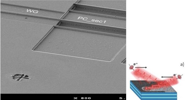
A waveguide device on InP that can manipulate passively the state of polarization. This is an essential building block in an optical circuit which uses mangetooptic interaction (Picture 1).
Kerr microscope image showing right- and left-circularly polarized laser pulses writing opposite magnetic domains while a train of laser pulses moves across a [Co/Pt]2 thin film (Picture 2).
Simultaneous strain and temperature fibre-based sensing using a laser based readout system
GRADUATION PROJECT: Simultaneous strain and temperature fibre-based sensing using a laser based readout system
Track: Connected World
Group: PhI
Mentor: Dr Erwin Bente and Stefanos Andreou
Context: Strain and temperature sensing and their real time monitoring are important for many applications. In particular for ASML lithography machines the wafer stages accelerate really fast and suffer small deformations which degrade the exposure quality. Lasers and Fibre Bragg Gratings (FBGs) are the two enabling tools for building such a sensing systems. Integrated lasers in particular and photonic integration in general are interesting because they can significantly reduce size and cost. The Photonic Integration group (PHI) develops InP based photonic integration technology by which lasers, photodetectors, amplifiers, splitters and other components can be monolithically integrated on a chip. FBGs are optical resonators inside an optical fibre. These are used as the transducers for detecting the desired strain and temperature since these shift their optical resonance frequency which can be monitored using a laser system. However, a well-known problem is the distinction between strain and thermal effects (often referred to as cross-sensitivity) which diminishes the system’s performance and resolution.
Brief system description and objective: In this project in collaboration with ASML the sensing system will use an integrated continuous wave ring laser the wavelength of which is locked to a π-shifted FBG using the so called Pound-Drever-Hall (PDH) frequency stabilization technique. PDH is a technique which uses the reflection of phase modulated light off an optical resonator structure (the FBG) to detect any wavelength drifts of the laser away from the optical resonance. This signal is used in an electrical feedback circuit that controls the laser frequency such that it stays at the optical resonance. The laser is thus locked to the FBG resonance and by applying axial strain or changing the temperature the resonance shifts and the wavelength of the laser as well. This wavelength can be measured accurately and the shift allows one to calculate back the strain or temperature change. The main objective of the project is to evaluate how well the strain and temperature effects can be decoupled. Different strategies can be deployed to perform this decoupling but in this project we would like to investigate mainly the one based on birefringent FBGs and polarisation diversity.
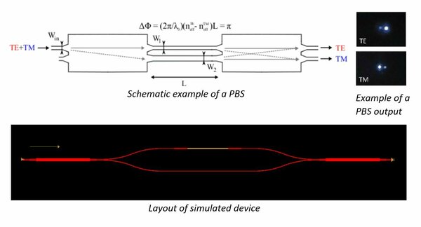
Design of a Tuneable Polarization Beam Splitter/Combiner in an InP-based generic platform
Track: Connected world
Group: PhI
Mentor: Stefanos Andreou (s.andreou@tue.nl) and Dr Erwin Bente (E.A.J.M.Bente@tue.nl)
Background: The polarization state of propagating light in photonic integrated circuits is an important property which can be exploited for various polarization diverse applications. Such can be polarization division multiplexing used in telecom which effectively doubles the available bandwidth or sensing applications where birefringence can be exploited in order to extract the desired quantity. Typically the light generated on-chip is Transverse Electric (TE) polarized. If one wants to take advantage of Transverse Magnetic (TM) polarization state as well we first need to covert TE state to TM using polarization rotators. Furthermore it is often desired that TE and TM modes co-propagate in the same waveguide or exit the chip from the same port which yields the need for the so-called polarization beam splitters/combiners (PBS).
Brief system description and objective: In this project the student is expected to come up with a design of a tuneable PBS in the InP-based generic platform that has been developed by our group using the already existing technology and designed components. The student will apply basic principles of photonics and use design/simulation tools (such as FDTD, BPM, etc) in order to determine the geometry of the device which will include passive waveguides, power splitters/combiners, phase modulators etc. Moreover, since for such integrated devices dimensions are critical, the device should include a tuning mechanism to compensate for fabrication imperfections which will be used to optimise the extinction ratio (the ratio between the power of TE and TM states) at the output of the device. Finally the student is also asked to perform a tolerance study for the proposed device. The duration of the project is 3 months, however if the student finds the topic interesting we can discuss for extending this internship project to a graduation project. The outcome of the project will be used in a system for strain and temperature system which deploys polarization diversity and other projects for which polarization handling components is relevant.