Semiconductor Nanostructures and Impurities
Research Profile
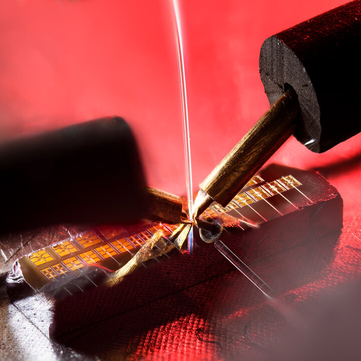
Individual semiconductor nanostructures and single impurities are offering interesting options to achieve and explore the ultimate limits in device miniaturization. Therefore we study the formation and electro-optic properties of individual semiconductor nano objects such as quantum dots, quantum rings and single impurities. To this end scanning probe techniques and atom probe tomography are used to determine the true 3D structure of various semiconductor nanostructures. By this we aim to understand and control their formation during growth and to link their structure to the electro-optic properties that we determine for instance by confocal microscopy. Scanning probe microscopy is furthermore used to explore and manipulate single (magnetic) impurities in a semiconductor material. This work has allowed for a deep understanding of quantum mechanical aspects that determine the properties of a whole range of impurities and defects in semiconductors.
News
![[Translate to English:]](https://assets.w3.tue.nl/w/fileadmin/_processed_/4/c/csm_Tjeertes%20Banner%20image_4bc0a85cfe.jpg "[Translate to English:]")

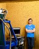
Meet some of our Researchers
Recent Publications
Our most recent peer reviewed publications
-
A.R. Da Cruz,R.S.R. Gajjela,P.M. Koenraad,Craig E. Pryor,Michael E. Flatté
Fine structure splitting cancellation in highly asymmetric InAs/InP droplet epitaxy quantum dots
Physical Review B (2024) -
E.G. Banfi,T.J.F. Verstijnen,E. Monroy,M.E. Flatté,P.M. Koenraad
Atomically resolved study of the unpinned GaN (10 1¯ 0) surface by cross-sectional scanning tunneling microscopy
Physical Review B (2023) -
T.J.F. Verstijnen,D. Tjeertes,E.G. Banfi,Q. Zhuang,P.M. Koenraad
Atomic scale analysis of N dopants in InAs
Physical Review B (2023) -
Jesse G. Park,David E. Jaramillo,Yueguang Shi,Henry Z.H. Jiang,Huma Yusuf,Hiroyasu Furukawa,Eric D. Bloch,Donley S. Cormode,Joel S. Miller,T. David Harris
Permanent Porosity in the Room-Temperature Magnet and Magnonic Material V(TCNE)2
ACS Central Science (2023) -
Stan E.T. ter Huurne,Adonai Rodrigues Da Cruz,Niels van Hoof,Rasmus H. Godiksen,Sara A. Elrafei,Alberto G. Curto,Michael E. Flatté,Jaime Gómez Rivas
High-Frequency Sheet Conductance of Nanolayered WS2Crystals for Two-Dimensional Nanodevices
ACS Applied Nano Materials (2022)
Contact
-
Visiting address
FluxGroene Loper 195612 AZ EindhovenNetherlands -
Postal address
Department of Applied PhysicsP.O. Box 5135600 MB EindhovenNetherlands -
Postal address
Department of Applied PhysicsP.O. Box 5135600 MB EindhovenNetherlands -
Secretary